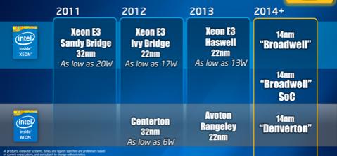
One of the more interesting pieces of information I overheard at SEMICON West earlier this month was that Intel 14nm was delayed. This rumor came from the semiconductor equipment manufacturers and they would know. What I was told is that the Intel 14nm process has not left the OR development facility to be replicated in the OR and AZ fabs.
Process move-in is an important milestone to product launch of course. 14nm move-in was supposed to happen in Q3 but it did not. I got an update this week and was told it would “probably” not happen until Q1. The speculation is that it is a “qualification delay”. I expected to hear something about it during the Intel Q2 2013 conference call but per the transcript:
“14 nanometer on-track to enter production by the end of the year” EVP and CFO Stacy J. Smith
“We are on track to start production on our 14 nanometer process technology in the back half of this year. CEO Brian M. Krzanich
“As far as our 14 nanometer Core launch in our – just our general product launch, I think what we’ve said so far is, first half of 2014 and we’re not going to – we’re not ready to give any specifics beyond that.” CEO Brian M. Krzanich
Maybe they will address it in the Q3 conference call on October 15[SUP]th[/SUP]. What is Intel 14nm exactly and how does it compare to the other 14nm offerings? Good question.
In planar process technologies the 28nm or 20nm implies the minimum transistor gate length of 28nm or 20nm. Corresponding to that lithographic capability are two other critical dimensions: the “contacted gate pitch” and the “metal pitch” for the lowest, thinnest metal layers. (Higher metal layers will be thicker with less resistance which are more suitable for longer routes but will have a greater width+space design pitch.) Given that, the 22nm and 14nm FinFET process technologies are a bit of a misnomer.
Intel opted for single patterning at 22nm (80nm first metal pitch), while focusing on introducing FinFET’s. At 14nm, they will pursue a ‘full’ node shrink, in the sense that they will be using double patterning and a 64nm first metal pitch.
The foundries took a risk in pushing for a 64nm first metal pitch at 20nm planar, with the requisite double patterning lithography. Both TSMC and GF will be maintaining a 64nm DPT metal pitch with their 16/14nm offerings. To read more about DPT see the Double Patterning Exposed articles from Mentor Graphics. They know DPT, believe it.
So, Intel pursued FinFET’s as a top priority, rather than DPT, keeping 22nm costs and risk down. TSMC and GF went DPT first at 20nm with thinner metals on a 64nm pitch and will add FinFETs as a “half” node one year later. A metal pitch of 64nm will be common between Intel, TSMC, and GF at 16/14nm. Both approaches accomplish the same objective but one may turn out to be more time/cost efficient than the other, time will tell.
It will be interesting to see what happens next year. Will Intel’s Haswell hit full production in 2014? What about Altera 14nmm FPGAs? And the SoC version of the Haswell? Delays are common place on bleeding edge semiconductor technology. Some companies own up to being human, some do not, but silicon does not lie.
The semiconductor industry is so close knit it is very hard to keep a secret. Add in social media and it is near impossible. I personally have 16,272 Connections on LinkedIn, linking me to 18,582,711+ professionals. I don’t know everything semiconductor but I certainly know someone who knows. I will keep working on verifying this rumor so stay tuned to SemiWiki.
Also Read: Intel Really is Delaying 14nm….
Share this post via:


Musk’s Orbital Compute Vision: TERAFAB and the End of the Terrestrial Data Center