The world is analog and despite enormous SoCs in the most leading-edge process node being the most glamorous segment of the semiconductor industry, it turns out that one of the fastest growing segments is actually analog and power chips in older process technologies. Overall, according to Semico, analog and power ICs, including discretes, are a $45B market today and growing at close to a 15% CAGR, faster than the overall semiconductor market.
 As a business, analog is especially attractive. Not just because it is growing faster than the overall semiconductor market, but also because, except for the most advanced mixed-signal SoCs (such as cell-phone modems), analog typically doesn’t use the most advanced semiconductor manufacturing technology. Accuracy rather than raw speed is typically what makes an analog design difficult. Analog design is more of an art than a science, with some of the smartest designers. This makes it impossible to move a design quickly from one fab to another or from one technology node to the next. So the analog business is characterized by long product cycles sometimes measured in decades.
In digital design, most of the differentiation in the product is in the design rather than in the semiconductor process itself. That is not true in analog where a good foundry can partner with its customers to create real value in the silicon itself. This will continue due to the increasing need for power-efficient analog, increased density and generally providing a higher quality product at lower cost.
Many markets that require a high analog and power content are heavily safety oriented. Most obviously, medical, automotive and mil-aero. This puts a premium on having solid manufacturing technology that can pass stringent quality and reliability qualification.
Further, there is increasingly a voltage difference between the SoCs that perform the major computation, which typically are running below 1V today, and the sensors, actuators, antennas and power supplies which require anything from 5V up to hundreds of volts. This creates an opportunity for analog using non-CMOS processes such as BCD (Bipolar-CMOS-DMOS) and for varieties that support even higher voltages for segments such as lighting, as the switch from incandescent to LED gradually takes place.
GLOBALFOUNDRIES addresses these markets with a platform-based product strategy accompanied with an investment strategy to put appropriate capacity in place to build a large scalable analog business. This is a part of its long-term strategic initiative called “Vision 2015.”
The two primary analog platforms are:
- 0.18um modular platform, with analog, BCD, BCDlite and 700V power
- 0.13um modular platform with analog, BCD and BCDlite
These platforms are modular in the sense that different capabilities can be added to a base platform depending on what devices are actually required in the final product, and especially how high a voltage is required to be supported. This creates a scalable manufacturing process that has flexibility to mix and match devices while at the same time being able to pass the highest standard qualifications. The modular aspect also enables manufacture at the lowest cost, only using fabrication steps that are actually required for the devices on that wafer batch.

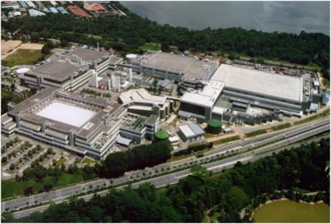
These analog platforms will run in Singapore in 200mm and 300mm fabs, which will also run 55nm and 40nm digital production.
GLOBALFOUNDRIES has already announced plans to strengthen its 300mm manufacturing capability in Singapore by increasing the capacity to be on a trajectory of nearly one million wafers per year. The expansion is planned to be complete by the middle of 2014.
I will be hosting a webinar on the analog and power markets, and the capital plans to support manufacture, on Tuesday April 9th. Join the webinar here. OOPS: forgot to say it is at 10am Pacific
Share this post via:


Musk’s Orbital Compute Vision: TERAFAB and the End of the Terrestrial Data Center