 I spent some quality time with Subi Kengeri, Vice President, Technology Architecture, Office of the CTO, GLOBALFOUNDRIES in Las Vegas during CES. Great guy, he worked at Silicon Access, Virage and TSMC before GF. One thing you should know about embedded memory guys, SRAM is the first thing that goes through a new process so they know their process technologies.
At Silicon Access Networks, Subi Directed a WW Engineering team to a first pass silicon sucess on industry’s first 10G classification processor SoC. At Virage, with responsibilities of WW design centers and advanced memory R&D, Subi took the Company to a leadership position on 90nm, 65nm and 40nm nodes. At TSMC, Subi was the Sr. Director in Design and Technology Platform and the Head of their North America Design Center. With a large engineering team in the US and Taiwan, Subi was responsible for technology enablement of advanced nodes and interfaced with strategic customers and partners.
Subi also has 30+ patents.
At GF, Subi is responsible for determining the technology feasibility, competitiveness and manufacturability of all elements of technology platform and to establish the advanced technology (14nm) roadmap. Subi is also one of the presenters at the Common Platform Technology Forum next week at the Santa Clara Convention Center:
[TABLE]
|-
| valign=”top” |
| valign=”top” | 2:50pm – 3:50pm
| valign=”top” |
| valign=”top” | Advanced Technology-Design-Manufacturing Co-optimization — A Triathlon
- Subramani Kengeri, Vice President, Technology Architecture, Office of the CTO, GLOBALFOUNDRIES
- Joe Sawicki, Vice President & General Manager, Design-to-Silicon Division, Mentor Graphics
This session explores the challenges of bringing advanced technology into high volume manufacturing. Similar to a Triathlon, there are three legs: Technology Architecture Development, Design Enablement and Manufacturing Ramp. Careful co-optimization of the interactions among all three disciplines is required at each stage of the process node maturity cycle. This technical session delves into critical requirements, challenges and solutions to enable SoC level product value and accelerated Time-to-Volume at current and future nodes, and touches on new approaches such as multi-patterning, FinFETs and IC reliability checking.
|-
Subi will start off with a quick overview of broad requirements that drive Foundry Technology which calls for deep collaboration with market drivers. Some areas of system design and technology collaboration will be discussed. Extending Mike Noonen’s point on changing landscape in the Mobile industry, Subi will touch upon the impact to foundry business and technology requirements before discussing details of two major challenges ahead: Device Architecture and Lithography.
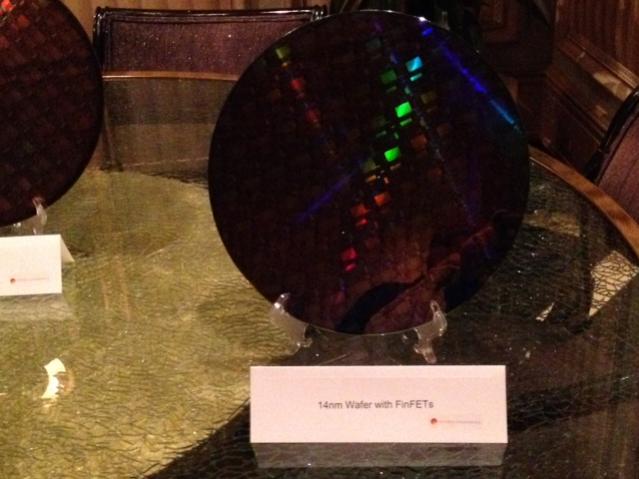
Next he will go into details of critical technology considerations for mobile applications with focus on power density and EM issues. He will explain the technology architecture options for reducing active and standby power in SoCs. This will lead into a discussion on why FinFET architecture requires very careful focus of parasitic modeling, EM-aware standard cell design and metrology to ensure optimization of critical SoC metrics and volume ramp. With first generation FinFET architected for time-to-volume, he will discuss how GF is leveraging their HKMG Production ramp. Further, all the SoC level optimizations done on 20nm planar, which gave it ~15% competitive area advantage, are being carried over to 14XM. He will show a comparison of critical metrics between 28nm, 20nm and 14XM that will highlight the key values of GLOBALFOUNDRIES offerings.
In the third section, Subi will go over 14XM development status and all the technology risk mitigation approaches we are using to bring up first generation FinFET into high volume quickly. Also, Subi will summarize ecosystem readiness for advanced technologies and then provide a view of the 10nm and 7nm technology roadmap. The talk will end with the importance of packaging technologies and show the GF roadmap for the next few generations.
I hope to see you there! Join me for lunch!


Musk’s Orbital Compute Vision: TERAFAB and the End of the Terrestrial Data Center