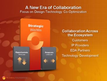
 GlobalFoundries did a nice response to my “How has 20nm Changed the Semiconductor Ecosystem?” and redefined the word collaboration. Our industry is plagued with sound bites and acronyms so let us agree on a semiconductor ecosystem definition of collaboration.
Mojy Chianis senior vice president, design enablement at GLOBALFOUNDRIES. He is responsible for global design enablement, services, and solutions and is the primary technical customer interface for the company. I have worked with Mojy for many years when he was at Conexant and Altera and have nothing but respect for him, especially when he buys me lunch. I finally got Mojy to blog and his first one “Re-Definig Collaboration” is right on the money, literally.
The concept of collaboration – when two or more partners take on a shared objective to meet a mutually defined and beneficial goal – is no longer optional if you are in the semiconductor business. Time, cost and complexity have made the ‘go it alone’ approach obsolete. On the manufacturing side, only a handful of companies have the wherewithal to bring next generation capacity on line because of unprecedented cost and difficulty.
I’m okay with that definition. Are you? Is there anything else to ad?
To address the chasm problem areas, an IDM-type interface is required between process teams at the foundry vendors and design teams at the fabless companies…A key issue is who establishes and pays for these IDM-type disciplines? Fabless company, foundry, or both? It is likely that many of the costs and disciplines will need to be shared.
I couldn’t agree more. I do believe however that the foundries are the driver and must lead the way on this. Meanwhile the fabless companies will continue to buy wafers based on price and delivery, right?
At the heart of collaboration today is a new type of relationship that borrows from the best of both the traditional IDM and foundry models. Our relationships with customers cannot be the ‘throw-it-over-the-wall’ approach that defined previous foundry models. We must be in lock step with customers’ internal strategies to the point that we both have skin in the game. Shared investment and success are hallmarks of collaboration in the modern foundry model.
Absolutely. Samsung calls it Simulated IDM. TSMC calls it Open Integration Platform (OIP). It will be interesting to see what label Mojy comes up with here.
In future posts in this space I will explore in more depth, from my vantage point of overseeing GLOBALFOUNDRIES’ design enablement efforts, key issues and approaches to enhancing efficiencies through collaboration throughout the ecosystem. These include how EDA and IP relationships must change, addressing critical requirements such as power and routability, silicon-verified design flows, DFM strategies, innovative technologies such as double patterning and HKMG, as well as some fundamentally new concepts like design-enabled manufacturing (DEM), which changes the perspective of where and how critical information is used to optimize the chip development process.
Now we are getting to the meat of the semiconductor sandwich! Foundry EDA and IP relationships MUST CHANGE! I will blog more on this later but I would like to hear from the crowd what really needs to be done here. Without design enablement we would not have design so let’s prioritize this to the highest level!
HOW DO THE EDA AND IP FOUNDRY RELATIONSHIPS NEED TO CHANGE?


Chemical Origins of Environmental Modifications to MOR Lithographic Chemistry