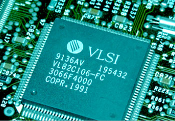
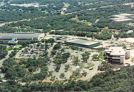
VLSI Technology was founded in 1981 by Dan Floyd, Jack Baletto and Gunnar Wetlesen who had worked together at Signetics. The initial investments were by Hambrecht and Quist, a cross between a VC and a bank, and by Evans and Sutherland, the simulation/graphics company.
The fourth person to join the company was Doug Fairbairn. He was still at Xerox PARC but went to interview the three founders for Lambda Magazine that he was just getting off the ground. He immediately realized that their plans for a foundry wouldn’t really work without a new generation of design automation tools because the EDA tools of that era were polygon-based layout editors but semiconductor technology was already past the point where you could reasonably design everything by hand.
 In the early days of VLSI, the company was sustained by designing ROMs for the first generation of video game consoles, which were all cartridge-based. Each cartridge actually contained a ROM with the video-game binary programmed into it. The fab in San Jose was not yet up and running, and so these were actually outsourced to Rohm in Osaka Japan. In parallel, Doug hired a bunch of PhDs, many from Carver Mead’s Silicon Structures Project at CalTech, and the profits from video games were invested in a suite of tools for what we would now call ASIC design, although that name didn’t come until later.
An early project, called Bagpipe, was to design a chip for the not-yet-announced Apple Macintosh. This chip had more sound channels and better graphics than the Mac eventually had, but Steve Jobs canceled the project in 1982 since he worried that finishing it might make the Mac late, which is actually laughable in retrospect since the Mac came out in 1984 at least a year later than planned in any case.
VLSI had a fab on McKay Drive in San Jose. At the time, it was the only high tech building there, surrounded by greenhouses growing flowers and, across the street was the Chrysanthemum Growers Association Hall that was sometimes used for company-wide meetings. The first process brought up was 3um HMOS, followed by 2um CMOS and 1.5um CMOS.
Fairly early on the investors decided that the company’s management team was too inexperienced to manage the anticipated growth. Al Stein was brought in as CEO. The company went public in February 1983, still not yet profitable, and almost immediately afterwards the 3 original founders departed.
The initial design technology, still based largely on the Caltech/PARC ideas in Mead and Conway’s seminal book Introduction to VLSI Design, was a mixture of manual design with generators for basic structures such as registers and adders using an internal language called VIP. The focus of the tools was on verification with a DRC, circuit extractor, LVS (called netcompare), simulators (VSIM, with no timing and then TSIM which had timing based on a simple capacitative model).
However, designs were getting too large for this approach and despite the inelegance compares to Mead and Conway’s ideas, it was clear that layout had to be much more automated. So standard cell libraries and a full place & route system were developed along with schematic capture to input the design.
In order to be successful, design had to get closer to the customer. Initially this meant that the customer came to VLSI and there were several teams working on site at VLSI’s San Jose buildings. For example, the main chip in France Telecom’s initial implementation of Minitel was created by Telic (now buried somewhere in Alcatel-Lucent) who sent a team of engineers from Strasbourgh to San Jose for several months.
The next step was to create a network of Design Centers (DCs) initially in the US, and then also in Japan and Europe, since it was clearly not scalable to bring all the customers on-site to California.
The IBM PC was now in its high growth phase and many customers of VLSI were designing products for that market (modems, add-in peripheral cards) or designing chips to create PC clones. In fact there were dozens of companies working with VLSI with a business strategy of being a large percentage of the PC industry, obviously an impossibility for all of them to succeed. To serve this market, VLSI developed the first of what today is called semiconductor IP although VLSI called them megacells (and later functional system blocks or FSBs). These included all the standard components in a PC such as the UARTs or the 6845 graphics controller.

Dan Yoder, as an experiment over a weekend, put all of these megacells together onto a few chips and created the first PC chipset, a chipset that could be used to create a full PC along with the Intel microprocessor and memory. VLSI ran with the idea and built up a large business in PC chipset standard products to go with its mainline ASIC business. One generation of chipsets was even resold by Intel.
Two key EDA products in the late 1980s were the datapath compiler and the state-machine compiler, effectively one of the first synthesis tools. The datapath compiler could take a complex description for a datapath and quickly generate a fully laid out datapath on silicon, using its own optimized custom library, not standard cells. And the state-machine compiler could take a description of a state-machine (or just any old logic) and produce an optimized implementation in standard cells. Together these two tools made creating complex designs much easier.
Share this post via:


Musk’s Orbital Compute Vision: TERAFAB and the End of the Terrestrial Data Center