TSMC 20nm is one of the most talked about nodes on SemiWiki with lots of speculation and debate surrounding it. It’s interesting to look back at what we thought would happen to see if it actually did happen so let’s do that now. According to Google there are 411 articles referencing 20nm on SemiWiki, let’s visit a couple of the… Read More
 Alchip’s Leadership in ASIC Innovation: Advancing Toward 2nm Semiconductor TechnologyAlchip Technologies has recently reported significant progress in…Read More
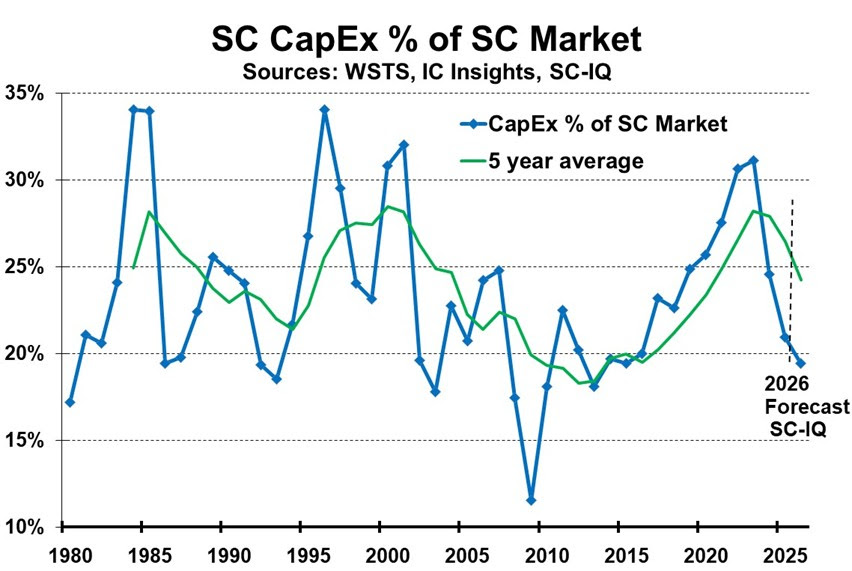 CapEx Up for Foundry, MemorySemiconductor Intelligence estimates total semiconductor industry capital spending…Read More
 RISC-V Now! — Where Specification Meets Scale!In forty plus years as a semiconductor professional…Read More
 Sensors Converge: Where Intelligence Meets the EdgeThe Sensors Converge Conference is one of the…Read More
Imec’s Process Secret Decoder Ring
To wrap up Semicon West, let’s go back to Monday and the imec presentations. In fact, An Steegen’s presentation titled The Semiconductor Roadmap. She covered a lot of ground, but some of her slides contain a wealth of information. Let’s look at the options for 10nm, 7nm and a little 5nm, what imec call N10, N7 and… Read More
GlobalFoundries: Upcoming Events
GlobalFoundries is running a series of technical seminars in the US and Europe, following on from the successful versions run last month in Shanghai and Hsinchu. Among the topics that will be discussed are Foundry 2.0 and Collaborative Device Manufacturing for both Leading Edge and Mainstream technologies. The European events… Read More
CEVA + Riviera Waves = Complete WiFi and BlueTooth Solution
Thanks to the recent acquisition of Riviera Waves, CEVA is expanding from Digital only DSP IP, to supporting complete solution (Digital + mixed-signal) for both WiFi and Bluetooth functions. Such a move is already a very good market positioning, as customers prefer buying to a single source the digital and the mixed-signal part… Read More
EDA Mergers & Acquisitions Wiki Now Includes IP
When I started collecting my list of EDA mergers and acquisitions about 30 years ago, my objective was simply to determine the number of logos each EDA company owns. For that reason, I collected all the fish-eat-fish-eat-fish…. mergers and acquisitions, going way back to the very early days of EDA (even before it was called EDA).… Read More
Intel 14nm Delayed Yet Again?
This week I’m at SEMICON West with 27,000 of my closest friends. Good information, good networking, and some great rumors this year. Yesterday I heard a juicy rumor in the halls that Intel is still having 14nm yield problems. Remember, we heard a similar rumor last year and it turned out to be true. I Googled around this morning and … Read More
Bob Metcalfe Keynote at #semiconwest
My PhD is in distributed file systems so one of the key networking papers was Metcalfe and Boggs, 1976. It was titled Ethernet: Distributed Packet Switching for Local Computer Networks. This was the paper that introduced the world to Ethernet and to Bob Metcalfe. He was on stage yesterday here at Semicon West to give the afternoon… Read More
Are iPhones to Die For?
First there were car phones and admittedly I waited in line to get one when they went mainstream. It was a Motorola something or other and it came with a curly antenna for the back window. From there I got a Nokia, a flip phone, a BlackBerry, and now iPhones. These life changing devices would not have happened without the fabless semiconductor… Read More
Chip side of the Open Interconnect Consortium
Maybe it’s my competitive analysis gene, or too many years spent hanging out with consortium types, but I’m always both curious and skeptical when a new consortium arises – especially in a crowded field of interest. The dynamics of who aligns with a new initiative, and how they plan to go to market compared to other entities, prompts… Read More
Mark Adams Keynote at #semiconwest
The first surprise of the opening keynote for Semicon West was on the slides that were cycling on the screen as the room filled up. Somehow our book Fabless had managed to be in the rotation.
The opening keynote was by Mark Adams, the President of Micron. He was talking about upcoming big changes in the semiconductor environment, although… Read More
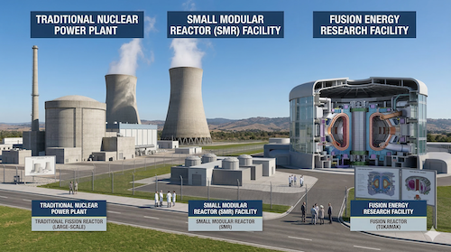
Musk’s Orbital Compute Vision: TERAFAB and the End of the Terrestrial Data Center