The world of AI algorithms continues to advance at a furious pace, and no industry is more dependent on those advances than automotive. While media and analysts continue to debate whether AI will deliver value in business applications, there is no question that it adds value to cars, in safety, some level of autonomous driving, … Read More
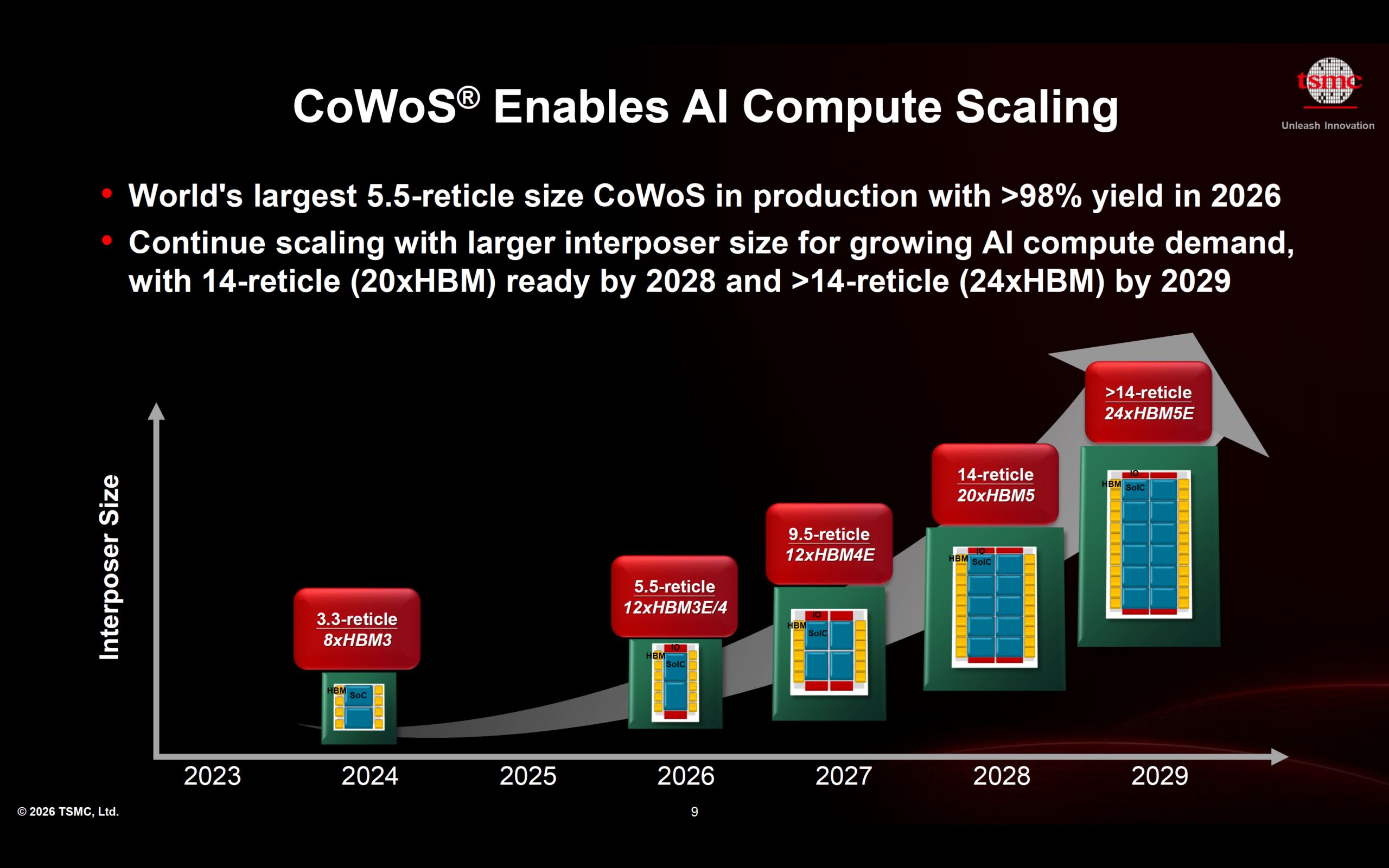
 Enabling Next-Generation AI Through Advanced Packaging and 3D Fabric IntegrationThe rapid rise of artificial intelligence is fundamentally…Read More
Podcast EP285: The Post-Quantum Cryptography Threat and Why Now is the Time to Prepare with Michele Sartori
Dan is joined by Michele Sartori – senior product manager at PQShield. Michele is a software engineer in Computer and Network Security, specializing in product management. He is a passionate tech team leader at the forefront of emerging technologies focused on achieving tangible results.
In this highly informative discussion,… Read More
Cost-Effective and Scalable: A Smarter Choice for RISC-V Development
The RISC-V ecosystem is witnessing remarkable growth, driven by increasing industry adoption and a thriving open-source community. As companies and developers seek customizable computing solutions, RISC-V has become a top choice. Providing a scalable and cost-effective ISA foundation, RISC-V enables high-performance… Read More
High-speed PCB Design Flow
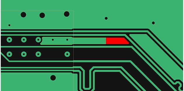
High-speed PCB designs are complex, often requiring a team with design engineers, PCB designers and SI/PI engineers working together to produce a reliable product, delivered on time and within budget. Cadence has been offering PCB tools for many years, and they recently wrote a 10-page white paper on this topic, so I’ll share … Read More
ESD Alliance Executive Outlook Features View of How Multi-Physics is Reshaping Chip Design and EDA Tools
Every spring, the ESD Alliance, a SEMI Technology Community, organizes a get together where industry executives and experts gather to network and talk about trends in the electronic design automation industry.
The theme of this year’s event, once again co-hosted by Keysight, is “How Multi-Physics is Reshaping Chip Design and… Read More
The Growing Importance of PVT Monitoring for Silicon Lifecycle Management
In an era defined by complex chip architectures, ever-shrinking technology nodes and very demanding applications, Silicon Lifecycle Management (SLM) has become a foundational strategy for optimizing performance, reliability, and efficiency across the lifespan of a semiconductor device. Central to effective SLM are Process,… Read More
TSMC Brings Packaging Center Stage with Silicon
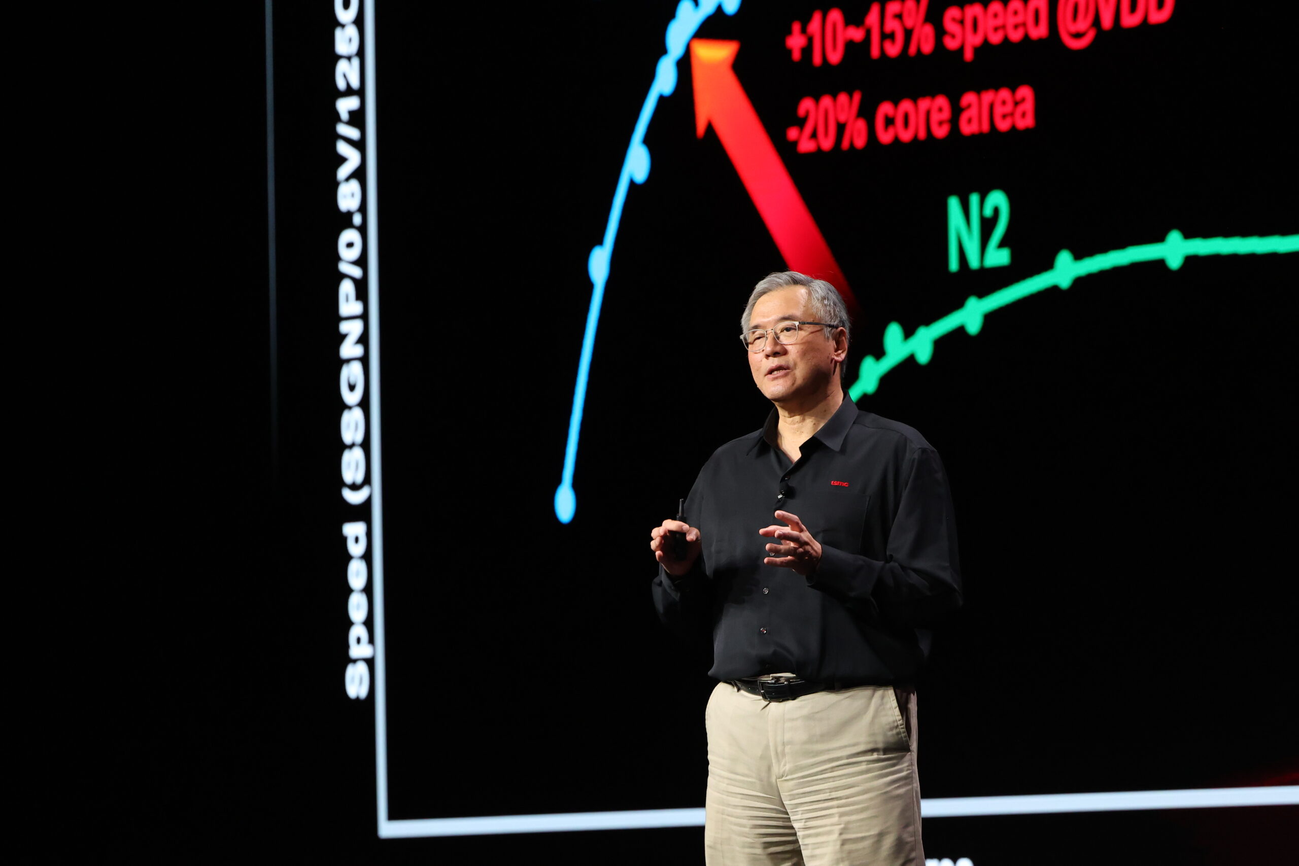
The worldwide TSMC 2025 Technology Symposium recently kicked off with the first event in Santa Clara, California. These events typically focus on TSMC’s process technology and vast ecosystem. These items were certainly a focus for this year’s event as well. But there is now an additional item that shares the spotlight – packaging… Read More
TSMC 2025 Technical Symposium Briefing
At the pre-conference briefing, Dr. Kevin Zhang gave quite a few of us media types an overview of what will be highlighted at the 2025 TSMC Technical Symposium here in Silicon Valley. Since most of the semiconductor media are not local this was a very nice thing to do. I will be at the conference and will write more tomorrow after the … Read More
Perspectives from Cadence on Data Center Challenges and Trends
From my vantage point in the EDA foxhole it can be easy to forget that Cadence also has interests in much broader technology domains. One of these is in data center modeling and optimization, through their Cadence Reality Digital Twin Platform. This is an area in which they already have significant track record collaborating with… Read More
Semiconductor Tariff Impact
President Donald Trump has initially excluded semiconductors from his latest round of U.S. tariffs. However, he could put tariffs on semiconductors in the future. If tariffs are placed on semiconductors imported to the U.S., how would that affect U.S.-based semiconductor companies? The chart below shows U.S. semiconductor… Read More


Solving the EDA tool fragmentation crisis