You are currently viewing SemiWiki as a guest which gives you limited access to the site. To view blog comments and experience other SemiWiki features you must be a registered member. Registration is fast, simple, and absolutely free so please,
join our community today!
Posts Search Results for "moortec"
Another year, another DAC, and last month it was #55DAC in SFO and the first thing that I noticed was that the event was no longer located in the traditional North or South Halls, rather we were in the smaller, Moscone West on two floors, almost like a 3D FinFET. Checkin to get my badge was highly automated and oh so fast, well done.… Read More
TSMC is the leading foundry worldwide and they make a big splash each year at the DAC exhibit and conference, so I stopped by their theatre area during the presentation from IP vendor Moortec to see what’s new this year. Stephen Crosher was the presenter from Moortec and we had exchanged emails before, so this was the first time… Read More
The TSMC OIP DAC Theater schedule is finalized and ready to go. It kicks off Monday at 10:15 am in booth #1629 and ends with a raffle at 5:45 pm each day (Mon-Tue-Wed) TSMC gives out some very nice prizes so check in with the TSMC booth staff when you arrive. There are 66 coveted presentation spots representing the top ecosystem partners… Read More
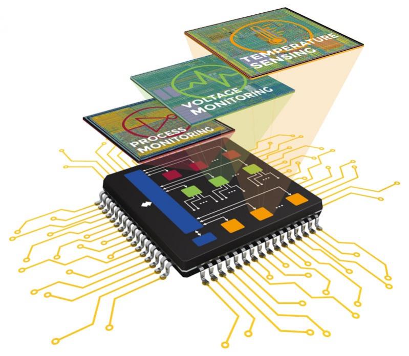
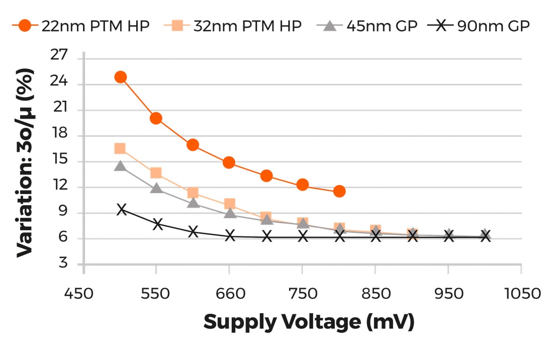
Have you ever wondered how process variation, thermal self-heating and Vdd levels affect the timing and yield of your SoC design? If you’re clock specification calls for 3GHz, while your silicon is only yielding at 2.4GHz, then you have a big problem on your hands. Such are the concerns of many modern day chip designers. To… Read More
In the old days to learn about new semiconductor IP you would have to schedule a sales call, listen to the pitch, then decide if the IP was promising or not. Today we have webinars which offer a lot less drama than a sales call, plus you get to ask your questions by typing away at the comfort of your desk, hopefully wearing headphones as … Read More
At Intel back in the late 1970’s we wanted to know what process corner each DRAM chip and wafer was trending at so we included a handful of test transistors in the scribe lines between the active die. Having test transistors meant that we could do a quick electrical test at wafer probe time to measure the P and N channel transistor… Read More
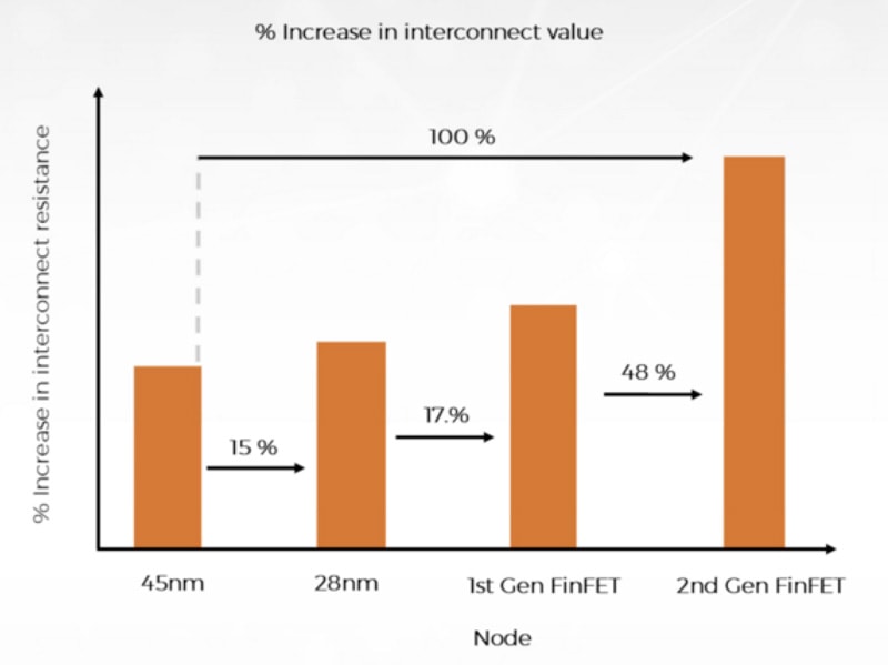
2017 was a banner year for semiconductor sales as they topped $400B for the first time, an increase of some 20%, there is happiness in Silicon Valley, Taiwan, South Korea, and well, everywhere. With the foundries pushing to ever-smaller process dimensions and even going back to mature nodes and offering more variations that are… Read More
Six years ago I first interviewed Stephen Crosher, CEO and Co-founder of Moortecas they were in startup mode with some new semiconductor IP for temperature sensing, and earlier this month I attended their webinar all about embedded in-chip monitoring to get caught up with their technology and growing success. Ramsay Allen is … Read More
In a former life I was the GM of a business where we built specialized structures used for semiconductor process bring-up, characterization and monitoring. These monitoring structures were placed in wafer scribe-lines and were used to monitor key parameters during wafer processing. The structures provided feedback to automated… Read More
Our smart phone driven semiconductor economy consumes a lot of IP blocks to enable quick product development cycles, often annually updating with new models to choose from. So where do you find all of the best semiconductor IP, verification IP and embedded software? Well, one place is at the 2nd annual REUSE conference, scheduled… Read More


Facing the Quantum Nature of EUV Lithography