
The patterning of features outside a DRAM cell array can be just as challenging as those within the array itself [1]. The array contains features which are densely packed, but regularly arranged. On the other hand, outside the array, the minimum pitch features, such as the lowest metal lines in the periphery for the sense amplifier (SA) and sub-wordline driver (SWD) circuits, are meandering in appearance, and the pitch is varying over a range. Stitched double patterning has been the method of choice but will not be sufficient when minimum pitch drops below 40 nm pitch [2,3]. Moreover, when the minimum pitch drops below 40 nm, EUV stochastic defectivity becomes an issue [4,5].
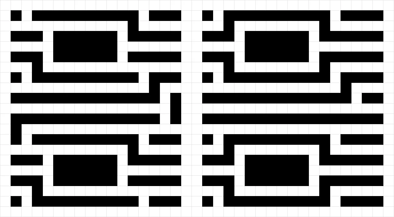
Self-aligned spacer patterning may be applied to the minimum pitch metal features in the DRAM periphery [6]. The sense amplifier and sub-wordline driver patterns are typically characterized by islands with minimum pitch lines meandering around them (Figure 1).

The wrapping of the lines around the islands does suggest similarity to the spacer wrapping around the core mandrel feature. Guided by the outline of the metal line directly wrapping around the islands, the appropriate mandrel features are shown in Figure 2.

The core is then removed, leaving the spacer (Figure 3).

The spacer acts as a mandrel for a second spacer, followed by filling of the remaining gaps (Figure 4). When necessary, cuts are used.

The patterning flow is similar to the self-aligned quadruple patterning (SAQP) used for pitch quartering [7]. Thus, for down to ~37 nm minimum metal pitches, this can be expected to allow DUV lithography to be used without the heavy processing burden of multiple litho-etch (LE) steps.
References
[1] F. Chen, Application-Specific Lithography: Sense Amplifier and Sub-Wordline Driver Metal Patterning in DRAM.
[2] F. Chen, Stitched Multi-Patterning for Minimum Pitch Metal in DRAM Periphery.
[3] S-M. Kim et al., “Issues and Challenges of Double Patterning Lithography in DRAM,” Proc. SPIE 6520, 65200H (2007).
[4] Y. Li, Q. Wu, Y. Zhao, “A Simulation Study for Typical Design Rule Patterns and Stochastic Printing Failures in a 5 nm Logic Process with EUV Lithography,” CSTIC 2020.
[5] F. Chen, Predicting Stochastic EUV Defect Density with Electron Noise and Resist Blur Models.
[6] F. Chen, Triple Spacer Patterning for DRAM Periphery Metal.
[7] H. Yaegashi et al., “Overview: Continuous evolution on double-patterning process,” Proc. SPIE 8325, 83250B (2012); DOI: 10.1117/12.915695.
Also Read:
FPGA Prototyping in Practice: Addressing Peripheral Connectivity Challenges
An Insight into Building Quantum Computers
I Have Seen the Future with ChipAgents Autonomous Root Cause Analysis
Share this post via:


Chemical Origins of Environmental Modifications to MOR Lithographic Chemistry