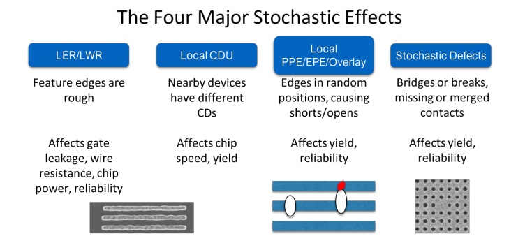
The relentless miniaturization of semiconductor devices has always relied on achieving ever-smaller features on silicon wafers. However, as the industry enters the realm of extreme ultraviolet (EUV) lithography, it faces a critical barrier: stochastics, or the inherent randomness in patterning at atomic scales. This phenomenon introduces variability that jeopardizes yields, reliability, and overall device performance, particularly as feature sizes shrink to the limits of EUV capabilities.
Understanding the Stochastics Challenge
Stochastics manifest in several detrimental forms: line-edge roughness (LER), linewidth roughness (LWR), local critical dimension uniformity (LCDU), and local pattern placement error (LPPE). These lead to edge placement errors (EPE) and, ultimately, stochastic defects—such as missing or bridging features—that can render entire chips defective. These issues, once minor when features were large, have grown in significance as feature sizes drop to sub-20 nm scales. For instance, a 2 nm LER on a 200 nm feature was negligible; on a 40 nm feature, it becomes critical.
The Stochastics Resolution Gap
A key insight introduced in the white paper is the Stochastics Resolution Gap: the difference between the resolution achievable in research labs versus what is viable in high-volume manufacturing (HVM). While 193i immersion lithography has largely closed this gap, EUV has not. Despite its theoretical capability to resolve features below 12 nm half-pitch, stochastic defects limit HVM production to ~16–18 nm. This ~4–6 nm resolution shortfall directly impacts chip area and cost, limiting the economic returns of EUV lithography.
Strategies to Lower the Stochastic Limit
To bridge this gap, the industry must lower the stochastic limit using various approaches:
-
Increase Exposure Dose: Raising photon counts reduces photon shot noise, but at the expense of throughput and cost. Since EUV photons are high energy and scarce, doubling the dose reduces variability only modestly while halving tool productivity—a costly tradeoff.
-
Resist Improvements: New metal-oxide resists (MORs) improve EUV absorption and reduce stochastic variation. MORs have shown promising results and are entering production, though optimization continues.
-
Etching Techniques: Innovations in atomic layer etching and deposition offer opportunities to smooth patterns and control dimensions post-exposure. These techniques can lower LER and improve LCDU, but their benefits vary by design.
-
Stochastics-Aware Design and OPC: Modern design rules now factor in stochastic variability, especially for critical layers. Likewise, optical proximity correction (OPC) must be calibrated using stochastic-aware models to prevent failure-prone “hot spots.”
-
Stochastics-Aware Process Control: Advanced metrology tools are needed to separate global and local variations and provide real-time control. Statistical process control (SPC) and advanced process control (APC) can be improved by using accurate measurements of stochastic effects.
The Role of Accurate Metrology
At the core of all these improvements lies measurement accuracy. Traditional scanning electron microscope (SEM) metrology often overestimates variability due to image noise, leading to biased and misleading results. Fractilia’s approach removes SEM-induced noise from the analysis, offering unbiased, high-precision metrology that reflects true wafer variability. This is essential for optimizing resist selection, refining etch recipes, generating design rules, calibrating OPC models, and improving process control.
Bottom Line
Closing the Stochastics Resolution Gap is critical to sustaining Moore’s Law and maintaining economic viability at advanced nodes. This requires coordinated advances in materials, process technologies, design practices, and—most importantly—stochastic metrology. By enabling accurate, real-world measurements, companies can better manage variability, improve yields, and accelerate ramp to production. Fractilia’s tools and methodologies represent a foundational step in enabling the next generation of semiconductor manufacturing.
The full white paper is available here.
Share this post via:


Intel, Musk, and the Tweet That Launched a 1000 Ships on a Becalmed Sea