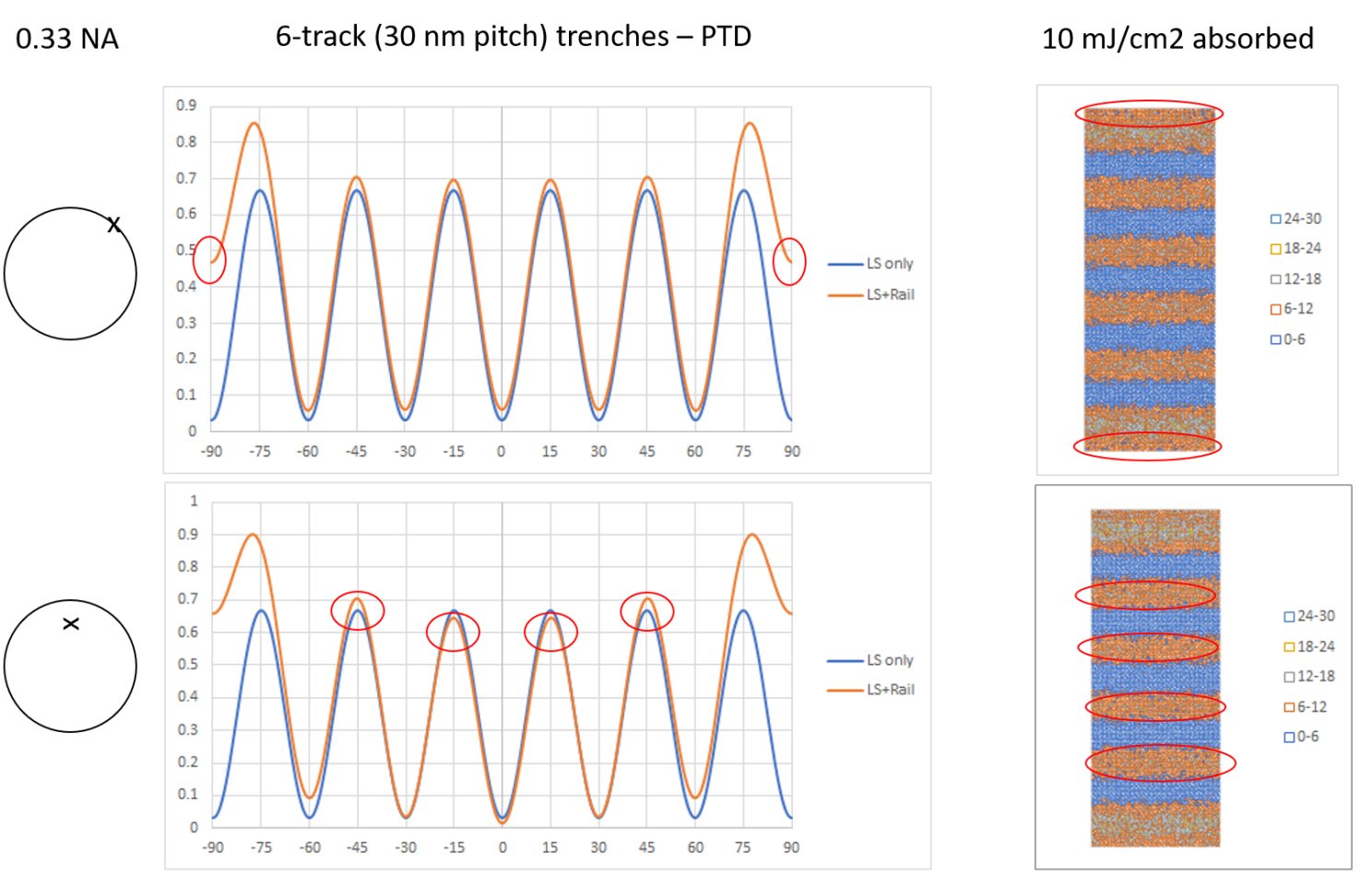
The discussion of any particular lithographic application often refers to imaging a single pitch, e.g., 30 nm pitch for a 5nm-family track metal scenario. However, it is always necessary to confirm the selected patterning techniques on the actual use case. The 7nm, 5nm, or 3nm 6-track cell has four minimum pitch tracks, flanked by larger width lines for ground and power rails. Figure 1 shows how a uniform 30 nm pitch exposure would lead to aggravated stochastic defect locations. When the illumination gives rise to fewer diffraction orders, a valley appears where we expect the rail peak, while image intensity imbalance occurs among the four inner trenches when more diffraction orders are included [1].

Figure 1. 30 nm pitch 6-track cell with exposed trenches (0.33NA EUV). The illumination angle (left) strongly affects both the optical image (center) and the expected stochastic defect location (right). The red circles indicate the stochastic defect hot spot locations.
When using a more absorbing metal oxide resist, unexposed trenches can be patterned. However, the aggravated stochastic defect locations are still present, and the image imbalance is worse, with pitch walking also evident (Figure 2).

Figure 2. 30 nm pitch 6-track cell with unexposed trenches (0.33NA EUV). The illumination angle (left) strongly affects both the optical image (center) and the expected stochastic defect location (right). The red circles indicate the stochastic defect hot spot locations. Red arrows indicate pitch walking (shift of peak positions).
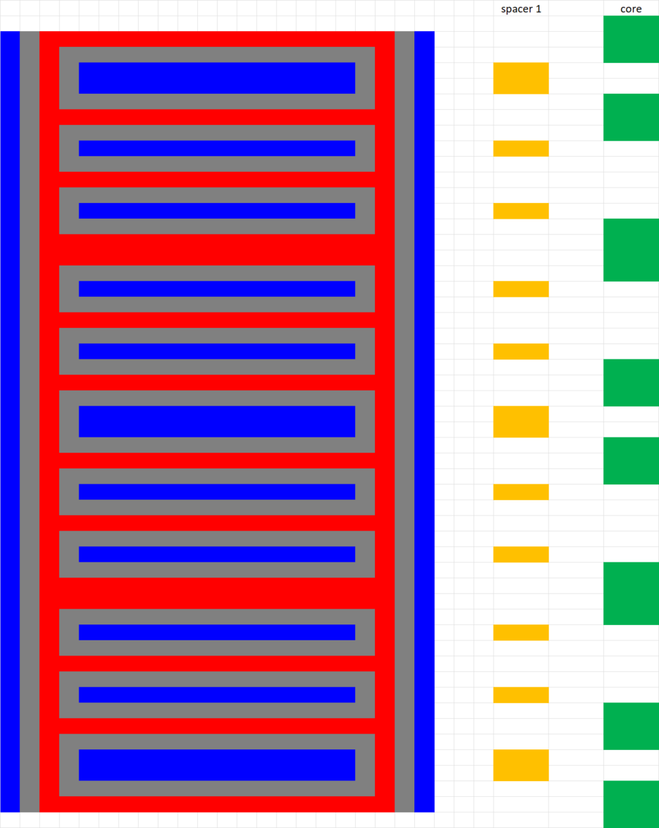
The High-NA EUV system does not change the outcome [1], and is also not available. To avoid the above issues, the only one-mask solutions for patterning four 30 nm pitch tracks with the two large rails would be EUV Self-Aligned Double Patterning (SADP) and DUV Self-Aligned Quadruple Patterning (SAQP), starting with the same core cell pitch. The EUV-DUV difference of complexity and cost far exceeds the SAQP-SADP difference of processing complexity and cost, since SAQP has already long matured on mature tools [2,3]. The expected spacer layout and arrangement for the SAQP approach are shown in Figure 3.

Figure 3. Spacer layout and arrangement for DUV SAQP for the 6-track cell. The blue and red lines would be cut or trimmed separately.
The SAQP would then be followed by applying a cut mask at least twice, each time on alternating lines. The same dual cut mask approach has been applied as part of the well-known Self-Aligned Litho-Etch-Litho-Etch (SALELE) approach used with EUV, which uses four EUV masks in total [4]. The LELE EUV masks may also be substituted by DUV LELE with SADP at lower cost, though up to 4 extra DUV masks may be needed [5].
References
[1] F. Chen, “6-Track Cell Imaging in Low-NA and High-NA EUV Lithography,” https://www.youtube.com/watch?v=Z9MQuKrqLYw
[2] L-A. Ragnarsson et al., “The Environmental Impact of CMOS Logic Technologies,” 2022 EDTM.
[3] L. Liebmann et al., The daunting complexity of scaling to 7NM without EUV: Pushing DTCO to the extreme,” Proc. SPIE 9427, 942702 (2015).
[4] R. Venkatesan et al., Direct print EUV patterning of tight pitch metal layers for Intel 18A process technology node,” Proc. SPIE 12292, 1229202 (2022).
[5] F. Chen, https://www.linkedin.com/pulse/extension-duv-multipatterning-toward-3nm-frederick-chen; F. Chen, https://www.linkedin.com/pulse/beol-mask-reduction-using-spacer-defined-vias-cuts-frederick-chen
This article first appeared in LinkedIn Pulse: Application-Specific Lithography: Avoiding Stochastic Defects and Image Imbalance in 6-Track Cells
Also Read:
Application-Specific Lithography: Sense Amplifier and Sub-Wordline Driver Metal Patterning in DRAM
Is Intel cornering the market in ASML High NA tools? Not repeating EUV mistake
Share this post via:


Musk’s Orbital Compute Vision: TERAFAB and the End of the Terrestrial Data Center