EUV lithography is a complicated process with many factors affecting the production of the final image. The EUV light itself doesn’t directly generate the images, but acts through secondary electrons which are released as a result of ionization by incoming EUV photons. Consequently, we need to be aware of the fluctuations of the electron number density as well as the scattering of electrons, leading to blur [1,2].
In fact, these secondary electrons need not be coming from the direct EUV absorption in the resist either. Secondary electrons can come from absorption underneath the resist, which include a certain amount of defocus. Moreover, there is an EUV-induced plasma in the hydrogen ambient above the resist [3]. This plasma can be a source of hydrogen ions, electrons, as well as vacuum ultraviolet (VUV) radiation [4,5]. The VUV radiation, the electrons and even the ions constitute separate blanket resist exposure sources. These outside sources of secondary electrons and other non-EUV radiation all basically lead to non-EUV exposures of resists in EUV lithography systems.
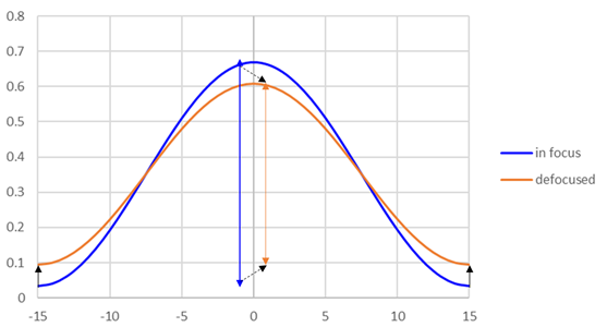
Defocused images have reduced differences between maximum and minimum dose levels, and also add an offset to the minimum dose level (Figure 1). Thus, when incorporated with the EUV-electron dose profile, the overall image is more sensitive to stochastic fluctuations, since the defocused doses are everywhere closer to the printing threshold. The blanket exposures from the EUV-induced plasma further increase sensitivity to stochastic fluctuations at the minimum dose regions.

Figure 1. Defocus reduces the peak-valley difference and adds an offset to the minimum dose level. This tends to increase vulnerability to stochastic fluctuations.
Thus, stochastic defect levels are expected to be worse when including the contributions from these non-EUV sources. The effect is equivalent to adding a reduced incident EUV dose and adding an extra background electron dose.

Figure 2. 30 nm pitch, 30 mJ/cm2 absorbed, 3 nm blur, without non-EUV sources. Pixel-based smoothing (rolling average of 3×3 0.6 nm x 0.6 nm pixels) is applied. Numbers plotted are electrons per 0.6 nm x 0.6 nm pixel.

Figure 3. 30 nm pitch, 40 mJ/cm2 absorbed, 3 nm blur, 33 e/nm^2 from non-EUV sources. Pixel-based smoothing (rolling average of 3×3 0.6 nm x 0.6 nm pixels) is applied. Numbers plotted are electrons per 0.6 nm x 0.6 nm pixel.
Figures 2 and 3 show that including non-EUV exposure sources can lead to prohibitive stochastic defects, regardless of where the printing threshold is set in the resist development process. In particular, the nominally unexposed regions are more vulnerable to the non-EUV exposure sources. The nominally exposed regions, on the other hand, are more sensitive to the dose levels and blur. The non-EUV exposure sources therefore contribute to providing a floor for stochastic defect density.
Thus, it is necessary to include the electrons emitted from underneath the resist as well as the radiation from the EUV-induced plasma as exposure sources in EUV lithography systems.
References
[1] P. Theofanis et al., Proc. SPIE 11323, 113230I (2020).
[2] Z. Belete et al., J. Micro/Nanopattern. Mater. Metrol. 20, 014801 (2021).
[3] J. Beckers et al., Appl. Sci. 9, 2827 (2019).
[4] P. De Schepper et al., J. Micro/Nanolith. MEMS MOEMS 13, 023006 (2014).
[5] P. De Schepper et al., Proc. SPIE 9428, 94280C (2015).
This article first appeared in LinkedIn Pulse: Non-EUV Exposures in EUV Lithography Systems Provide the Floor for Stochastic Defects in EUV Lithography
Also Read:
Application-Specific Lithography: Sense Amplifier and Sub-Wordline Driver Metal Patterning in DRAM
BEOL Mask Reduction Using Spacer-Defined Vias and Cuts
Predicting Stochastic Defectivity from Intel’s EUV Resist Electron Scattering Model
Share this post via:


Musk’s Orbital Compute Vision: TERAFAB and the End of the Terrestrial Data Center