As verification continues to be a key ingredient in successful design implementation, new approaches have been tried to balance cost, time to results and comprehensive analysis in designs that require large patterns in some application like Image Processing. Simulation environments are well proven, and designers tend to use approaches they are familiar with, but these tend to take a lot of time for large verification suites. FPGA prototyping provides improved runtimes but setting up the targeting flow takes time. Emulation provides significant acceleration, but this comes at a hefty cost.
Vaxel Inc, a Silicon Valley startup, provides a verification approach that blends nicely the Simulation, FPGA synthesis and Emulation methodologies and it calls it Verification Acceleration (thus the name Vaxel). It is a low-cost software solution that is FPGA target agnostic and it automates the steps in FPGA targeting, allowing the designer to choose their preferred FPGA vendor and then allowing a 10X-30X improvement in runtime at a much cheaper cost than emulation. (Disclosure: I am helping Vaxel in Design Enablement and I am part of the organization).
Note that VAXEL is NOT an FPGA based prototyping tool but is a block level verification acceleration tool.
Yasu Sakakibara, Vaxel Inc CTO has published a paper entitled ‘Image Processing Verification beyond Simulation, Emulation, FPGA synthesis’.
In this paper, he examines the benefits and limitations of each verification approach (summarized by drawing excerpts here from the paper):
Simulator
A Simulator is without a doubt the verification tool that is most widely used in chip development projects. On one hand, it provides a large degree of latitude and helps you construct a verification environment where you can check operations closely by viewing waveforms and performing highly flexible input/output simulations. On the other hand, its operation speed is devastatingly slow. Therefore, you need creative approaches to the verification environment to compensate for the slowness. The following are examples:
- Bypassing some of the time-consuming and repetitive processes, such as initial settings.
- Adding some debug functions to the HDL design where verification can be performed with downsized input data.
- Preparing a set of specific verification data that is likely to extend to “boundary conditions” with a reduced amount of data.
- Executing “backdoor” memory initialization and dump.
These approaches will speed up a Simulator, but the downside is that they all lead to more complicated configuration procedures and more cumbersome code maintenance.
Emulator
While a conventional Emulator can perform high-speed verification because it is constructed with dedicated hardware to perform an HDL operation, the first and foremost issue with the Emulator is its cost. It is a very powerful tool and the capabilities are vast. But, the license for both initial deployment and the subsequent renewals is extraordinarily expensive. Because of this, Emulators are usually shared among multiple projects, even within the largest OEMs in the industry. Not only from the economical viewpoint, but also from the verification procedure viewpoint, an Emulator requires you to prepare behavior models to substitute peripheral functions. This is also time-consuming work.
Design verification on an Emulator can often result in a poor perspective in terms of error correction due to the discovery of block-level bugs that were not caught in the previous process using the Simulator because of those cutting-corners approaches you took to compensate for the slowness.
FPGA Prototyping
FPGA Prototyping is an effective low-cost verification method compared to an Emulator. However, to effectively prepare the dedicated hardware requires extensive knowledge of FPGA. In many cases, an FPGA specialist is assigned to the project in addition to the design engineer and the verification engineer. As a result, the benefit of FPGA Prototyping diminishes rather quickly.
The following illustrates other problems that need to be addressed with FPGA prototyping:
- The speed difference between onboard DRAM on FPGA and DUT.
- The necessity of RTL modification specifically for FPGA to run DUT at high speed.
- The observability of internal states.
- Defining the transfer method of input and output data.
- Determination of a control method for the FPGA board.
- That preparation of the FPGA board can be a time-consuming and costly project itself.
The Verification Acceleration Value Proposition
The ideal verification acceleration tool should come with a ready-to-use set of standard hardware function IP blocks, such as bridges and interfaces so that the setup would be easy and fast. The tool should be affordable, and that it should require little expertise in FPGA.
To accomplish the above, the following should be the elements and requirements of a 4[SUP]th[/SUP] way solution:
- A software package available on the Internet that users can easily download, install and use.
- Support standard off-the-shelf FPGA evaluation boards for low-cost deployment.
- Utilize an embedded processor inside the FPGA for controls to provide “visibility”.
- Use HDL native features for waveform generation and assertion settings
- Deploy an operation scheme and structure similar to those of the Simulator
- An interface to allow the Simulator to execute simulation on the tool.
- Migration assisting tool from the verification environment set up on the Simulator
- Automated FPGA synthesis script generator so that little expertise in FPGA is needed.
- Includes CPU libraries to manage the verification environment.
- Support USB for host-board communication.
- Verification processes are run by firmware on the embedded processor inside FPGA by a command from the host.
- Support commonly used programming language libraries such as C and Python as well as CLI, so that test data generation can be done by non-HDL design engineers.
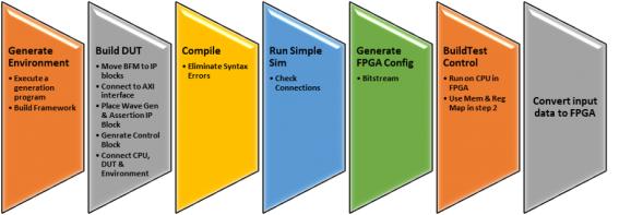
The paper details the approach taken to verify an Image Processing design with large test patterns in three steps:
1. Run a smoke test on the simulator
2. Confirm connection to the simulator

3. Conduct verification on the FPGA
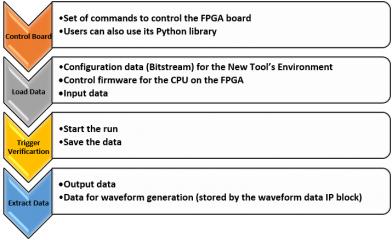
Controlling the FPGA board, loading firmware to the CPU on FPGA, and transmitting and extracting the input/output data are all done by the host PC.

The 4th way seems to find a way optimizing cost, time and block functionality checking with automation and acceleration.
Share this post via:


Captain America: Can Elon Musk Save America’s Chip Manufacturing Industry?