In a fresh development, Intel Corporation's chief commercial officer and general sales manager has announced his resignation. Intel reported the move through an SEC filing earlier today and shared little details behind his departure except for the effective date of the resignation and the reason behind it. According to the firm, the departing executive, Christopher Schell, will resign on June 30th. Intel has yet to announce his replacement, and the departure comes after the new CEO, Lip-Bu Tan, made customer satisfaction a key tenet of his turnaround strategy at Intel.
Intel's Chief Commercial Officer & General Sales Manager Will Leave Company In June
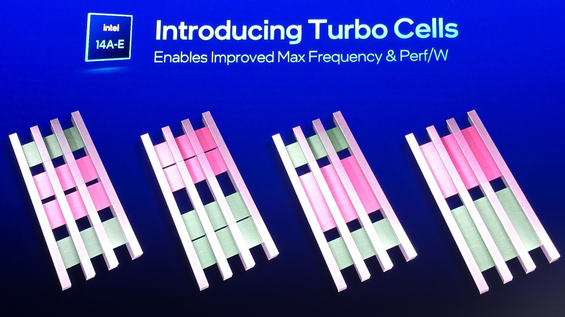
Schell's departure comes after Intel's foundry event in California yesterday, which saw the firm confirm that its leading-edge 18A manufacturing process is on track for delivery in 2025. 18A is Intel's response to TSMC's N2 process technology family, and the Taiwanese firm is expected to start mass production with the new technology in 2025 as well.
Like TSMC, Intel aims to target the contract chip manufacturing market. However, at the foundry event, the firm revealed that the 18A process would be limited to some high-performance computing (HPC) applications. HPC refers to large-scale computing applications such as analytics and AI and uses advanced processors, unlike those found in consumer personal computers.
Intel also revealed a new technology node called the 18A-P. This variant will target general applications, such as consumer chips. It will be available in 2026.
Intel's latest foundry process roadmap. Image: Intel Corporation
Since Intel plans to attract commercial customers to its foundry division, the role of a commerical officer and sales manager will be expanded as well. Previously, the only commercial sales of its products were either to retailers or to businesses using server chips. Intel's manufacturing struggles have also led it to bleed server market share to smaller rival AMD, making the role of a commercial officer even more important.
Customer satisfaction is a key priority of Intel's new CEO Lip-Bu Tan. Immediately after he took over, Tan, in his first message to Intel employees,
stressed that the firm's customers were counting on it to execute successfully. By focusing on customer satisfaction, Tan asserted that Intel would, in turn, generate shareholder value.
While its foundry event yesterday was highly anticipated, investors, it seems, are waiting for concrete execution. Intel's shares are down by 3% in morning's trading today. In an analyst note after the event, investment firm Cantor Fitzgerald kept a Neutral rating and a $26 share price target for the firm. Cantor didn't hear "meaningful surprises" at the event, but it was assured by Tan setting "down a market from which [it could] judge performance in the weeks, months, and years ahead." The firm added that concrete details about potential foundry customers, such as NVIDIA and Broadcom, would also be a meaningful development.
Chipmaker Intel's chief commercial officer and general sales manager will leave the firm by June end it says in an SEC filing.

wccftech.com