On the Sunday evening at IEDM last year, TechInsights held a reception in which Arabinda Das and Jeongdong Choe gave presentations that attracted a roomful of conference attendees.
This is the second part of the review of Jeongdong’s talk, we covered NAND flash technology in the last post. Jeongdong is a Senior Technical Fellow at TechInsights, and their subject-matter expert for memory technology. Before joining the company, he worked as a Team Lead in R&D for SK Hynix and Samsung advancing next-generation memory devices, so he knows whereof he speaks.
DRAM Technology
First up in the DRAM part of the talk was the roadmap:
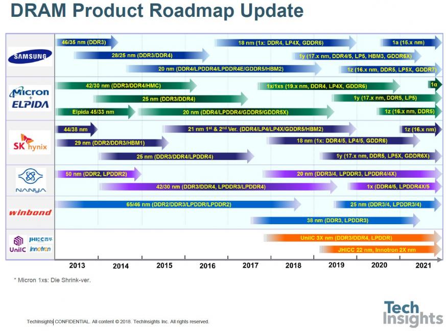
We are now well into the 1x-nm generations, with 17-nm parts being introduced this year. If you believe the manufacturers, we are still on the one-year cadence for introduction of the next shrink, although the difference is smaller, now we are below 20 nm. A few years ago, I was inclined to think that we might get two generations in the 1-something nodes before the technology reached its limits, but now it seems we will see at least four, which will likely see us through to 2025 at least.
The slowing of the shrink rate is shown by looking at the chronological trend of the nodes:
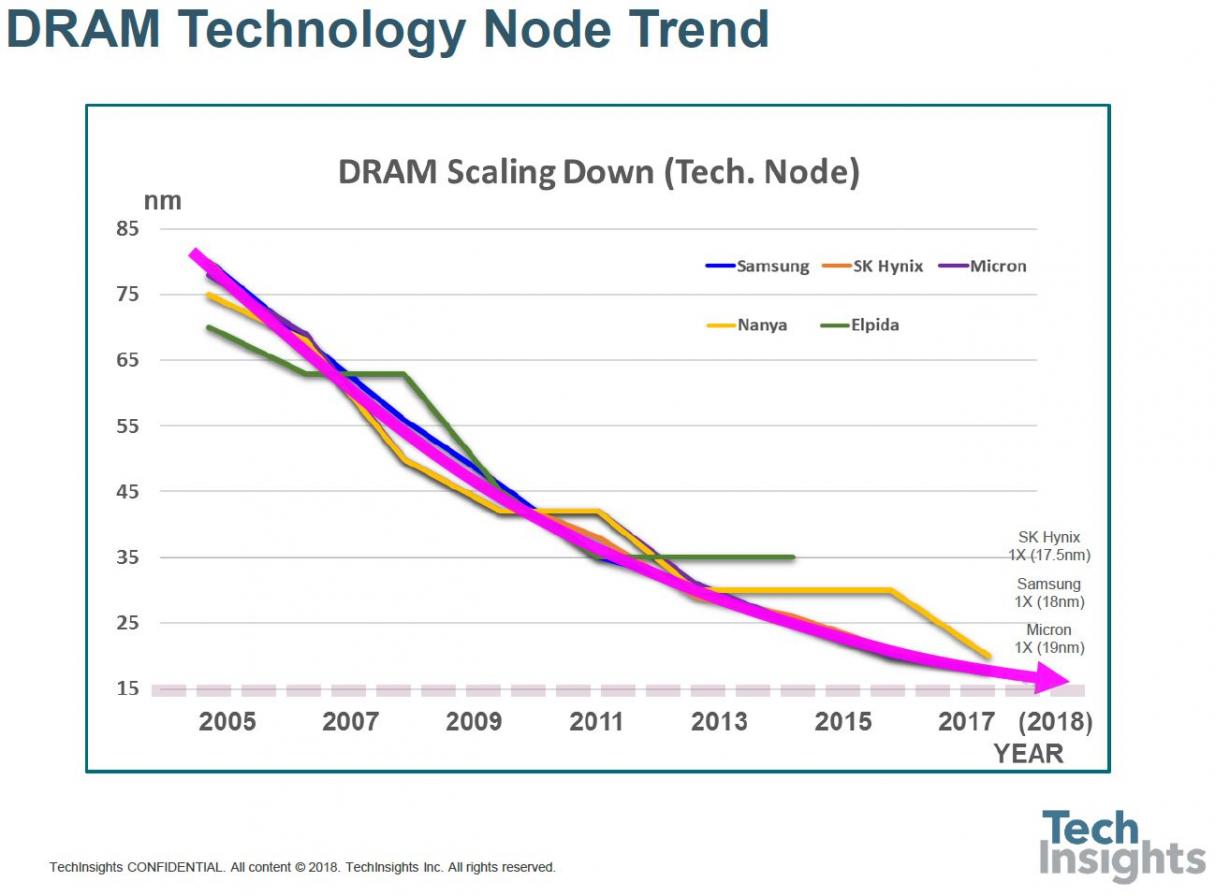
Elpida plateau-ed before the Micron acquisition, as did Nanya.
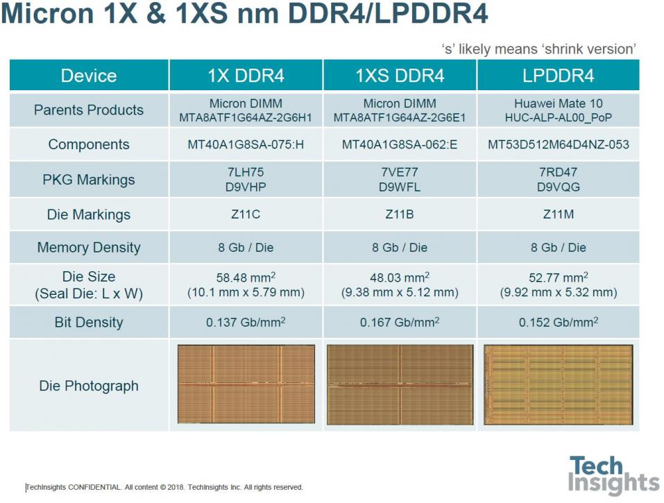
Jeongdong also gave us some details of recent Micron memories, showing that in 8-Gb dies their bit density is now up to 0.167 Gb/mm[SUP]2[/SUP].
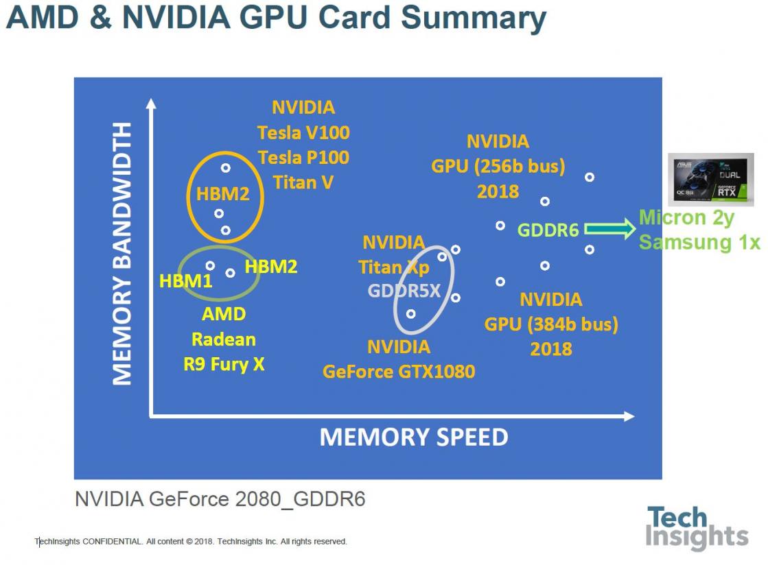
Then a look at AMD and Nvidia GPUs, illustrating the increase in bandwidth with the use of HBM (high bandwidth memory) and HBM2, and both bandwidth and speed as we move from GDDR5X to GDDR6.
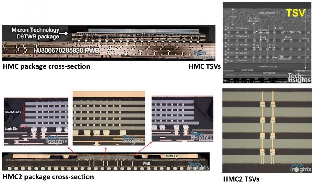
The mention of HBM brings to mind Micron’s HMC (Hybrid Memory Cube), which has now evolved into HMC2. The original HMC was used in the Intel Knight’s Landing processor, a four-stack DRAM with an IBM-fabbed controller chip at the base, connected with through-silicon vias (TSVs). HMC2 seems to have been was launched as an independent product, but still a 4-stack with controller, and both HMC and HMC2 used 30-nm class DRAMs.
Both HBM and HMC use TSVs, but they are different beasts; HMC has its controller die and is fully packaged for mounting on a PCB substrate, whereas HBM is used with a silicon interposer. However, Micron has announced that it is discontinuing HMC, so even though we got a look at it, it will not be around for much longer.
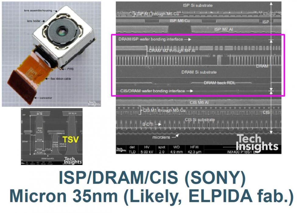
The last slide of the DRAM section covered the stacking of DRAM with CMOS image sensors (CIS) and processors (ISP) for mobile phone cameras, by Sony and Samsung. In the Sony IMX400 a DRAM is sandwiched between the CIS and the ISP; the CIS is mounted face-to-back on the DRAM, which is face-to-face with the ISP. Having the DRAM in the stack allows the camera system to perform at 960 frames/sec, serious slow motion capability. The IMX400 was launched in the Sony Experia XZ phones, and we published a blog on it at the time.
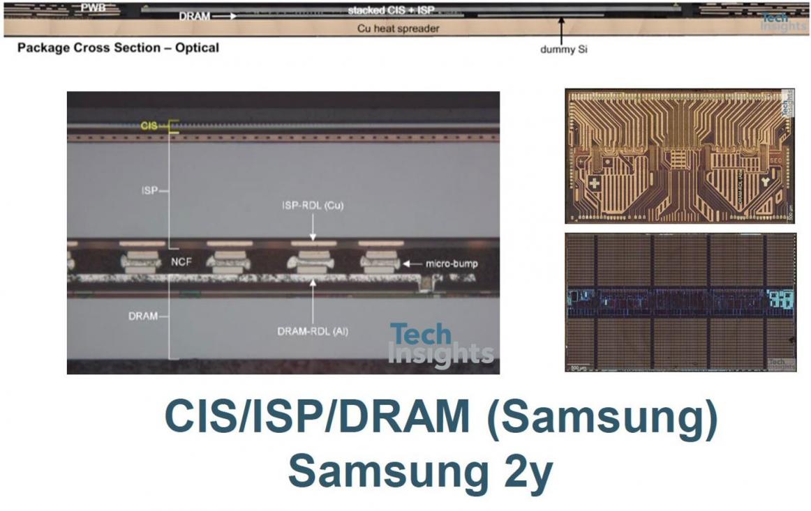
The Samsung S5K2L3 ISOCELL Fast imager takes a different tack – the CIS and ISP are conventionally bonded face-to-face and electrically connected using TSVs, and a standard DRAM chip is micro-bumped face-to-back on the ISP. The micro bumps connect a redistribution layer (RDL) on the DRAM to a Cu-based RDL on the back of the ISP, which routes them to TSVs, through the ISP substrate to the front metal. There is also a dummy silicon die next to the DRAM chip.
Emerging Memory Technology
Jeongdong finished his talk with a review of emerging memories – though how “emerging” some of them are is up for debate, since some products have been around for a while now. Here’s the roadmap:
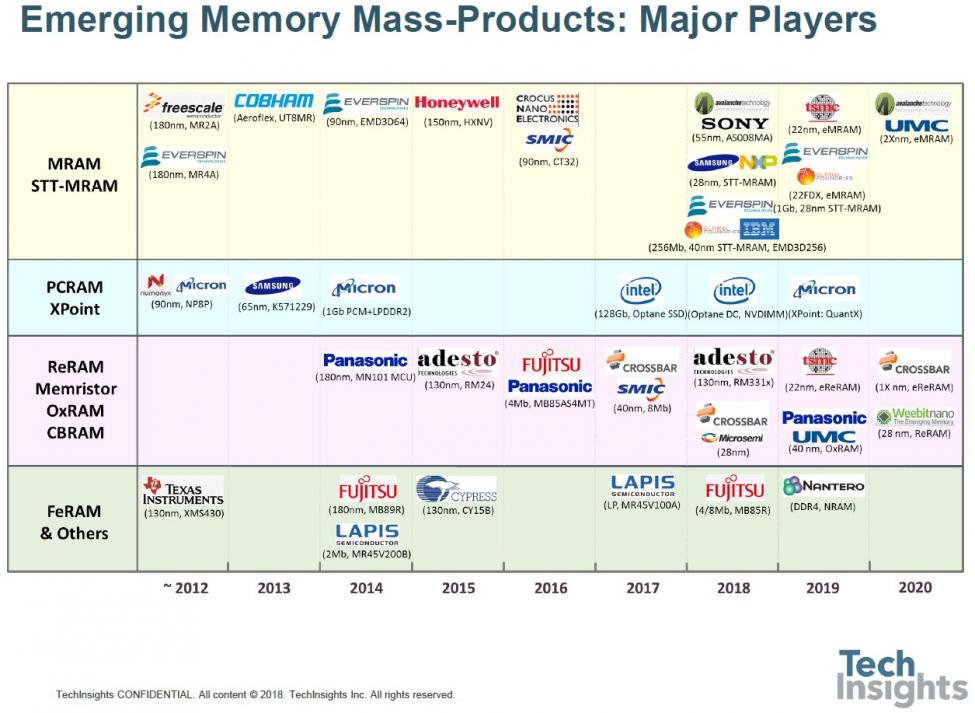
For example. Everspin has been making MRAM of various sorts for a while now, phase-change memory (PC-RAM) has been trialed on numerous occasions by a number of companies, and Fujitsu has been shipping its FeRAM for years.
The first example was the Adesto CBRAM (conductive bridge RAM), detailing the change between their first- and second-generation CB memories.
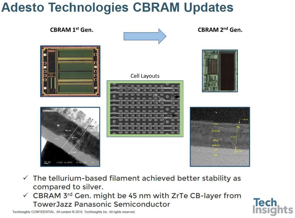
Structurally, the bridge layers have changed from silver/germanium sulphide to a tellurium-based multi-layer stack, which I presume is less temperature-sensitive than the silver.
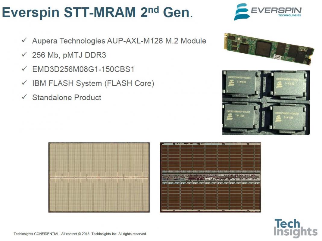
Then we were shown the 256-Mb Everspin 2[SUP]nd[/SUP]-gen STT-MRAM, using perpendicular-MTJ (magnetic tunnel junction) technology in a DDR3 format.
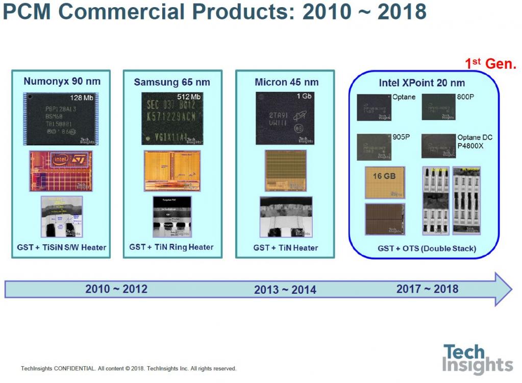
As a lead-up to the 3D-Xpoint slides which completed the talk, we were reminded that PC memory has been around for a while, and we have gone from 128 Mb from a 90-nm process to 20-nm 16 Gb:
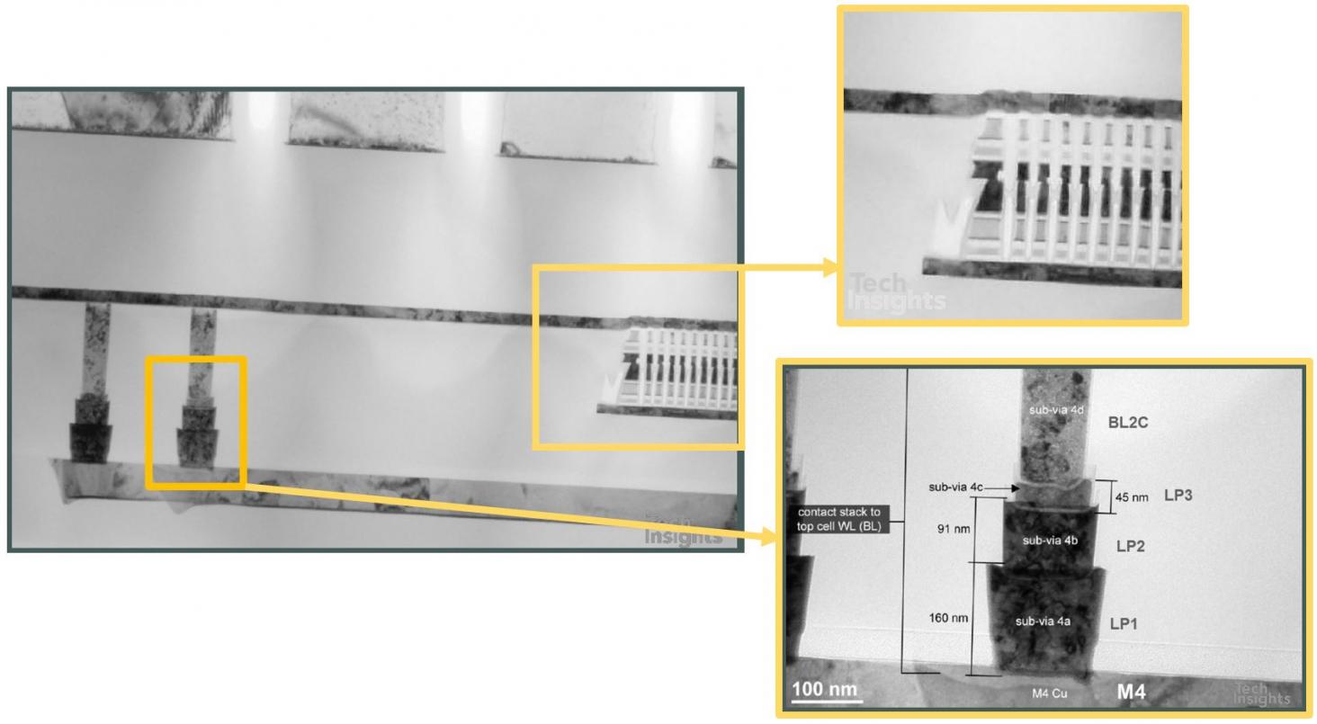
It appears that, at least in the Intel Optane version of 3D Xpoint, there are dummy memory blocks at the memory level (i.e. between metals 4 and 5), which have no drive circuitry, so that the circuit area is different from the memory array area. There are also structural differences in the double stack of the memory cells; in the lower cells it appears that the storage and selector layers are missing (though there are enough shadows of them in this image that the disappearance could be a sample-prep artefact). However, the tungsten wordlines in the centre are clearly separated.
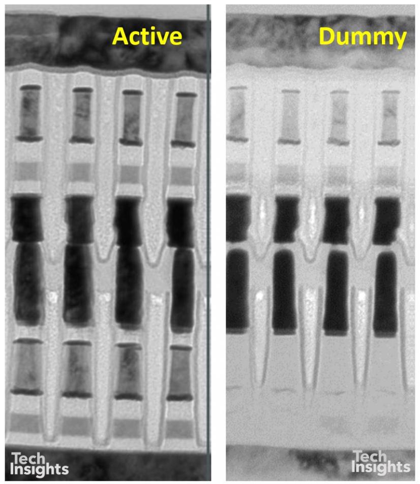
This stacking of the two layers of course adds to the process complexity, since we have to double up the deposition, etch, and photo steps; and in the bottom layer the wordlines are at the top of the stack, whereas the top stack has the wordlines at the base – and the reverse for the bitlines.
Adding the memory layers between M4 and M5 provides other challenges to the via structure between those layers, requiring more mask layers and the associated cost. The upper wordlines and bitlines are actually connected from below; as an example, the bitlines have a stack of four sub-vias to get up to the top bitline level.
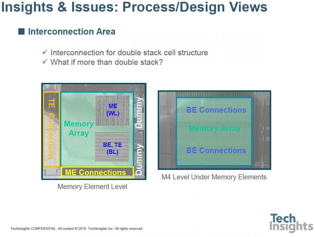
In plan-view it looks just as complex, so this poses the question – what do we do if we want to go to more than a double-stack structure? (BE/ME/TE = bottom/middle/top electrodes.)
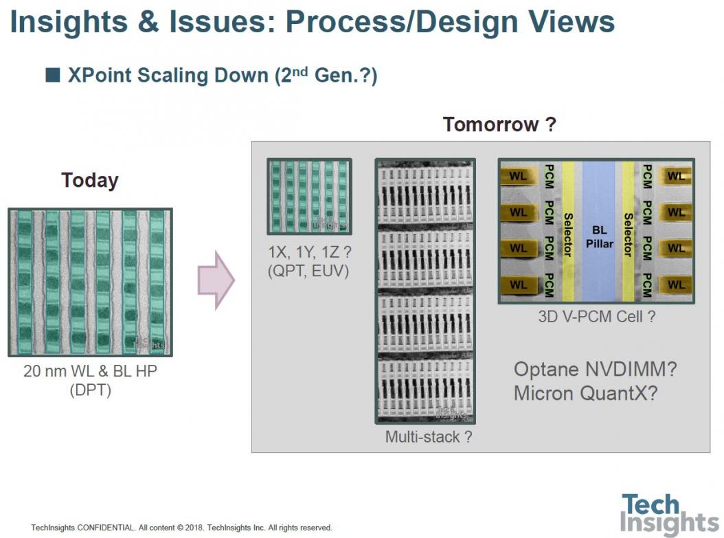
At the moment double patterning is being used, but of course there is the prospect of going to quadruple patterning, or even EUV, and maybe a multi-stack or 3D structure:
That concluded the talk, but don’t forget that all of this information, and a lot more, is available through the Memory Subscription from TechInsights.
Share this post via:


Musk’s Orbital Compute Vision: TERAFAB and the End of the Terrestrial Data Center