Nvidia has gained exclusive access to TSMC’s upcoming A16 semiconductor process, according to reports. The two companies are now running joint tests on the A16 process, which features nanosheet transistors and Super Power Rail technology. Nvidia is expected to use the A16 node for its next-generation Feynman GPU architecture, slated for release in 2028.
Food for thought
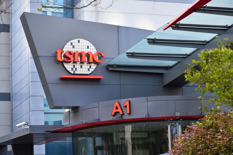
Implications, context, and why it matters.TSMC A16 timing strains Nvidia 2028 Feynman
- A16 enters risk production in 2026, an early low volume trial to prove yield and manufacturability, with volume late 2026 and 2027 1. Nvidia must hit 2028 Feynman.
- The node adds 8–10% performance and drops power 15–20% vs N2P 1. SemiWiki lists OpenAI, AMD, and Nvidia on A16 1, so exclusivity looks like early access.
- Second generation GAAFET nanosheet transistors plus backside power delivery that TSMC markets as Super Power Rail cut IR drop, which is unwanted voltage loss along power routes, enable tighter routing and raise cost which can limit early yields for large GPUs 1 2.
Packaging and HBM supply shape AI accelerator rivals
- Equipment makers with OSATs (Outsourced Semiconductor Assembly and Test providers) spot an opening in TSMC’s CoWoS (Chip‑on‑Wafer‑on‑Substrate) bottleneck, as Nvidia reserved 70% of 2025 CoWoS‑L capacity.
- TSMC is building CoPoS, a panel level advanced packaging approach, plus it plans wafer scale packaging that will need new tooling and partners.
- HBM3E sits at 12 high, while HBM4 may reach 16 high with hybrid bonding that uses direct copper to copper interconnect, more likely in HBM4E 4. A16 class GPUs need more TSV (Through‑Silicon Via) lines and better thermal control.
- Hyperscalers with chip startups sit behind TSMC CoWoS supply. That chokepoint keeps HBM4 memory suppliers near Nvidia, so building alternative packaging lines or moving to vertical integration, which means owning more of the design to manufacturing stack, can cut reliance.
