Array
(
    [content] => 
    [params] => Array
        (
            [0] => /forum/threads/nvidia-gets-exclusive-access-to-tsmc%E2%80%99s-a16-chip-process.23929/
        )

    [addOns] => Array
        (
            [DL6/MLTP] => 13
            [Hampel/TimeZoneDebug] => 1000070
            [SV/ChangePostDate] => 2010200
            [SemiWiki/Newsletter] => 1000010
            [SemiWiki/WPMenu] => 1000010
            [SemiWiki/XPressExtend] => 1000010
            [ThemeHouse/XLink] => 1000970
            [ThemeHouse/XPress] => 1010570
            [XF] => 2030770
            [XFI] => 1060170
        )

    [wordpress] => /var/www/html
)

Nvidia gets exclusive access to TSMC’s A16 chip process

Daniel Nenni

Admin
Staff member
1761860194685.png


1736840503_shutterstock_2276649193-750x500.jpg


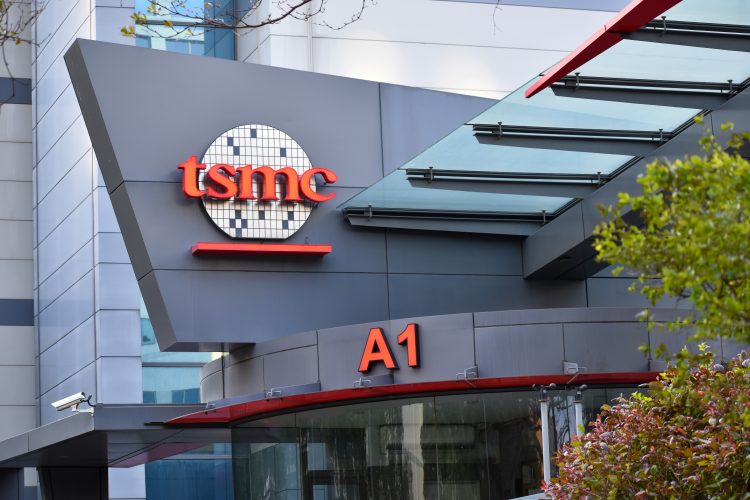
Nvidia has gained exclusive access to TSMC’s upcoming A16 semiconductor process, according to reports. The two companies are now running joint tests on the A16 process, which features nanosheet transistors and Super Power Rail technology. Nvidia is expected to use the A16 node for its next-generation Feynman GPU architecture, slated for release in 2028.

Food for thought​

Implications, context, and why it matters.

TSMC A16 timing strains Nvidia 2028 Feynman​

  • A16 enters risk production in 2026, an early low volume trial to prove yield and manufacturability, with volume late 2026 and 2027 1. Nvidia must hit 2028 Feynman.

  • The node adds 8–10% performance and drops power 15–20% vs N2P 1. SemiWiki lists OpenAI, AMD, and Nvidia on A16 1, so exclusivity looks like early access.

  • Second generation GAAFET nanosheet transistors plus backside power delivery that TSMC markets as Super Power Rail cut IR drop, which is unwanted voltage loss along power routes, enable tighter routing and raise cost which can limit early yields for large GPUs 1 2.

Packaging and HBM supply shape AI accelerator rivals​

  • Equipment makers with OSATs (Outsourced Semiconductor Assembly and Test providers) spot an opening in TSMC’s CoWoS (Chip‑on‑Wafer‑on‑Substrate) bottleneck, as Nvidia reserved 70% of 2025 CoWoS‑L capacity.

  • TSMC is building CoPoS, a panel level advanced packaging approach, plus it plans wafer scale packaging that will need new tooling and partners.

  • HBM3E sits at 12 high, while HBM4 may reach 16 high with hybrid bonding that uses direct copper to copper interconnect, more likely in HBM4E 4. A16 class GPUs need more TSV (Through‑Silicon Via) lines and better thermal control.

  • Hyperscalers with chip startups sit behind TSMC CoWoS supply. That chokepoint keeps HBM4 memory suppliers near Nvidia, so building alternative packaging lines or moving to vertical integration, which means owning more of the design to manufacturing stack, can cut reliance.
 
Cutting edge AI generated news. :ROFLMAO:

Tech in Asia (YC W15) is the largest English-language technology media company that focuses on Asia. From the latest news to the hottest trends and the boldest startups to the strongest titans, we cover everything tech in the region. Our goal is to build and serve Asia’s tech and startup community. In January 2024, Tech in Asia became a member of The Business Times.
 
View attachment 3820

1736840503_shutterstock_2276649193-750x500.jpg


Nvidia has gained exclusive access to TSMC’s upcoming A16 semiconductor process, according to reports. The two companies are now running joint tests on the A16 process, which features nanosheet transistors and Super Power Rail technology. Nvidia is expected to use the A16 node for its next-generation Feynman GPU architecture, slated for release in 2028.

Food for thought​

Implications, context, and why it matters.

TSMC A16 timing strains Nvidia 2028 Feynman​

  • A16 enters risk production in 2026, an early low volume trial to prove yield and manufacturability, with volume late 2026 and 2027 1. Nvidia must hit 2028 Feynman.

  • The node adds 8–10% performance and drops power 15–20% vs N2P 1. SemiWiki lists OpenAI, AMD, and Nvidia on A16 1, so exclusivity looks like early access.

  • Second generation GAAFET nanosheet transistors plus backside power delivery that TSMC markets as Super Power Rail cut IR drop, which is unwanted voltage loss along power routes, enable tighter routing and raise cost which can limit early yields for large GPUs 1 2.

Packaging and HBM supply shape AI accelerator rivals​

  • Equipment makers with OSATs (Outsourced Semiconductor Assembly and Test providers) spot an opening in TSMC’s CoWoS (Chip‑on‑Wafer‑on‑Substrate) bottleneck, as Nvidia reserved 70% of 2025 CoWoS‑L capacity.

  • TSMC is building CoPoS, a panel level advanced packaging approach, plus it plans wafer scale packaging that will need new tooling and partners.

  • HBM3E sits at 12 high, while HBM4 may reach 16 high with hybrid bonding that uses direct copper to copper interconnect, more likely in HBM4E 4. A16 class GPUs need more TSV (Through‑Silicon Via) lines and better thermal control.

  • Hyperscalers with chip startups sit behind TSMC CoWoS supply. That chokepoint keeps HBM4 memory suppliers near Nvidia, so building alternative packaging lines or moving to vertical integration, which means owning more of the design to manufacturing stack, can cut reliance.

I don't think Google, Amazon, Microsoft, Qualcomm , or even Apple have any interest to own, develop, or operate advanced packaging business.

"Hyperscalers with chip startups sit behind TSMC CoWoS supply. That chokepoint keeps HBM4 memory suppliers near Nvidia 5, so building alternative packaging lines or moving to vertical integration, which means owning more of the design to manufacturing stack, can cut reliance."

There is no reason for them to do it. Zero. TSMC can build packaging facilities in concert with fabs so this should not be a choke problem. Materials might be a problem but manufacturing capacity will not. Who better to know packaging capacity needs than the company who will manufacture the wafers? Exactly.

I remember when the rumor was Apple would build their own fabs. That was a good one. Apple is going to have a big iPhone 17 update cycle, GOT TSMC!
 
Back
Top