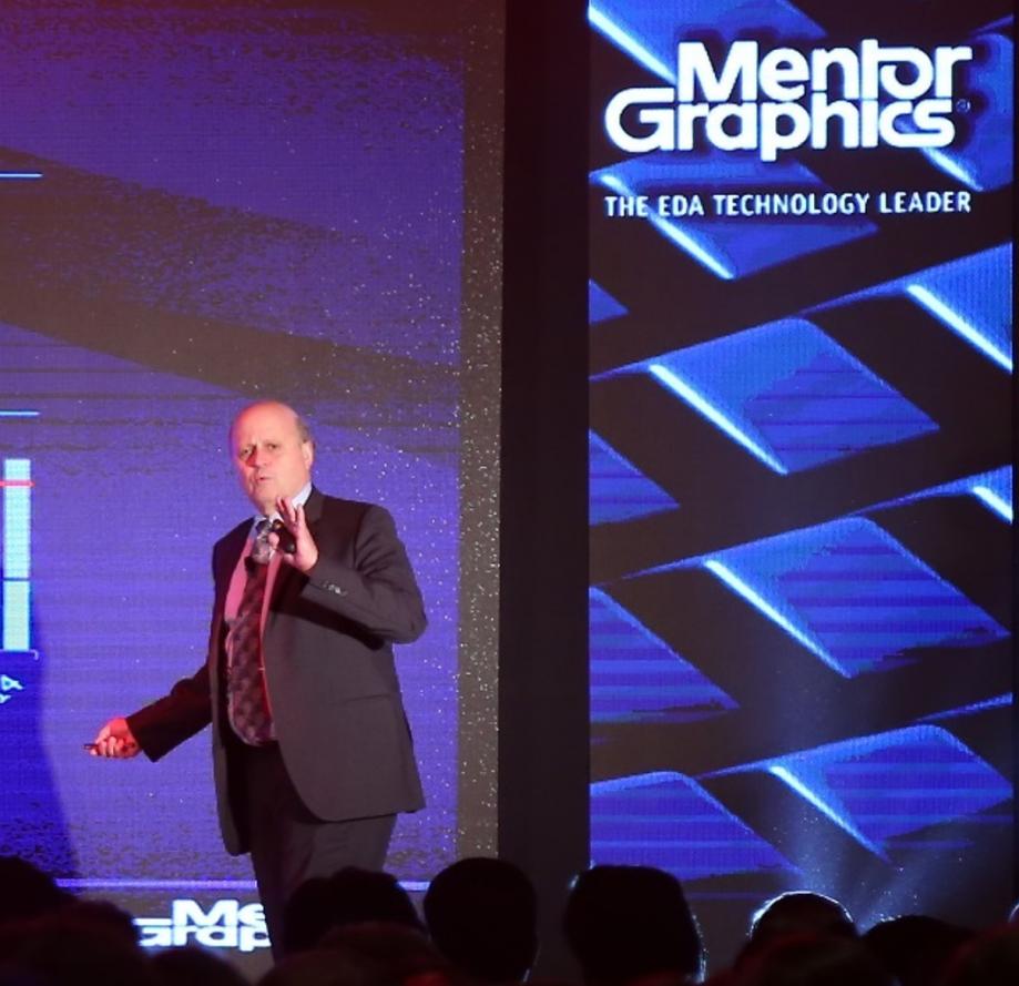
In a semiconductor industry which appears maturing, we are also seeing the technologies unravelling newer transistor structures, memories, processors, and newer ways of designing ICs and electronic systems. The present decade appears to be at the cusp of a new transformation in the semiconductor industry. Amid a slew of mergers and acquisitions this year, multiple questions arise on how these will affect or shape the future of semiconductor industry.

Dr. Walden C. Rhines, Chairman and CEO of Mentor Graphics Corporationpresented a keynote in their 11[SUP]th[/SUP] User2User India Conference. In his keynote titled “Merger Mania” Dr. Rhines emphasized about the major change in the structure of the semiconductor industry that will affect everything from the product definition to its design and manufacturing. I found a great opportunity talking with Dr. Rhines and getting his perspective on some of the key issues I thought will be coming in the way as we transition into the new phase of the semiconductor industry along with these mergers. Here is the conversation –
Q: Dr. Rhines, a large number of mergers this year reminds me about 2008 when the global financial crisis took place. Although the main cause of that crisis was housing subprime mortgages, there was also a significant consolidation in the semiconductor and other arena just before 2008. How do you interpret the current consolidation? Are we expected to see some sort of financial crisis again in coming years?
A: I hope there will not be a crisis like 2008; at that time housing loans by a large number of people could not be paid back. Today, the situation is not like that. There is liquidity in the market, credit is available at cheap interest rates, and there is free market economy. This is favouring debt and hence acquisitions and mergers are practical because they provide better economy of scale. At the same time the government tries to bring equilibrium in the economy whenever there is distortion in the market. So when interest rates start increasing the merger activities will slow down.
Q: In the current consolidation we are seeing multiple elements. The cost and capital conservation are anyway there to an extent, but there is innovation and expansion as well in particular areas such as IoT and its related segments. Do you see this consolidation bringing a bigger business opportunity rather than just contraction in the number of companies?
A: I see the opportunities in several ways. The corporate overhead will reduce and more money will be available for R&D and innovation. This is a periodic cycle; when acquisition happens, there is reduction in spending, but new businesses expand in due course of time. On the average 14% of the semiconductor revenue goes into R&D. So there may be more expansion in coming years, of course the law of economics cannot be violated.
Q: How do you see the fabless and IP model of business being impacted amid this consolidation?
A: The percentage of IC revenue from foundry wafers continues to increase; it’s touching to about 40%. The silicon foundries have enabled competitive costs for fabless companies, thus enabling economy of scale for IC production. So there may be a few IDMs acquiring fabless companies, but overall the fabless business will continue to grow. Among IP, the standard IP like USB or PCIe are commoditized. However the other value-added IP business will continue to grow.
Q: In near future we can foresee major changes coming in terms of transistor technologies, memories, processing power, IC manufacturing etc. and all of that at nominal cost to end-user. How is the semiconductor industry preparing to cope with providing high-value at lower cost?
A: The cost of transistor has decreased since last 50 years through reduction in feature size. Now wafer cost reduction is reaching its limits, but the transistor cost can still go down by increasing volume and other new technologies to reduce cost. There can be multiple dies in the same package. There is a learning curve associated with every new technology, so in due course we will see new technologies evolving and there will be further growth in the semiconductor industry.
Q: The technology is the driver for EDA tools and EDA tools are enablers for designs. The technology also brings new paradigms in designs. How do you see the EDA tools evolving amid new demands from the technology and design arena?
A: The EDA is an exciting field. Today it caters to multiple prominent process nodes – 28nm, 20nm, 14nm, 10nm, and now 7nm is close to stabilizing. The modern EDA tools are factoring multiple aspects in the design phase of ICs, e.g. manufacturing, cost, yield, and so on. The correlation of test failure with layout is evolving as a significant business. The cost reduction has to be achieved through multiple means. The systematic defects have to be automatically identified through the use of data mining and analysis.
About 5 years ago, Emulation was applied to only graphics chips, but today it’s used to verify any big digital chip. The Emulation driven verification business has doubled in last 3 years. The verification incurs largest expense in a design. The verification cost has to be reduced by multiple means. In the coming future, there will be many changes in EDA tools to enable more efficient design and verification in multiple ways.
Q: China is investing huge money to develop semiconductor industry in that region; M&A is also a part of that initiated by Chinese institutions. How do you see the worldwide semiconductor industry from regional perspective?
A: Yes, in China, the government along with private equity (PE) corporations have announced a five year plan to invest in big way in semiconductors (foundry as well as fabless) which will involve development in China as well as acquisitions in foreign countries. The government will invest ~$20 billion and PEs will invest ~$100 billion. We have already seen the acquisitions of Spreadtrum, STATS ChipPAC, ISSI, OmniVision, and Montage Technology. Micron’s acquisition is proposed for $23 billion. So, there will be a significant development in the semiconductor industry from China, stimulated by PE investment there.
Q: After more or less 35 prime years of semiconductors, we are seeing our second generations just entering this fascinating industry which infuses semiconductors in most of the other industries. What is your message to our younger generation engineers who may see a much transformed semiconductor industry than we saw?
A: The best is yet to come. So far we have seen many styles of chips in the form of ICs, now SoCs. Going forward system design will be in the mainstream. Design and verification is still in infancy. Although large designs are being developed, the verification is still being done in the same way as we were doing 30-40 years ago. We have to think in terms of system design from the beginning; define, implement and verify at that level.
Q: This is Mentor’s 11[SUP]th[/SUP] U2U conference, similar events are happening in other EDA companies. Considering these initial years of this century as pivotal for next generation semiconductor industry, what is the most important observation in the design community you think should be continued or changed?
A: The semiconductor industry is a learning industry; it needs a lot of collaboration and interaction. Today there are many ways of sharing information across the world through internet, webinars, tele-conferences, and so on. However, the design engineers still require direct physical interaction. So, focused User2User and other technical conferences are the best forums for sharing and learning. There is no end to these conferences, they will continue. The attendance in U2U conferences keeps increasing; we hold U2U conferences in all user dominated regions across the world.
It was a very inspiring discussion with Dr. Rhines. We eagerly look forward to the best yet to come in the semiconductor industry!
Pawan Kumar Fangaria
Founder & President at www.fangarias.com


Comments
0 Replies to “Merger Mania: The Future of the Semiconductor Industry”
You must register or log in to view/post comments.