

3D IC was a very popular topic at DAC. The era of heterogeneous, multi-chip design is here. There were a lot of research results and practical examples presented. What stood out for me was a panel at the end of day two of DAC that was hosted by Siemens. This panel brought together an impressive group of experts to weigh in on what was really happening and what the future looked like. I thoroughly enjoyed the honest and direct comments from this group. In case you missed it, there is a link coming so you can experience the whole event. To set the stage, here is a short summary of the excellent discussions about scaling 3D IC technologies as Siemens hosts a meeting of the minds at DAC.
The Distinguished Panel
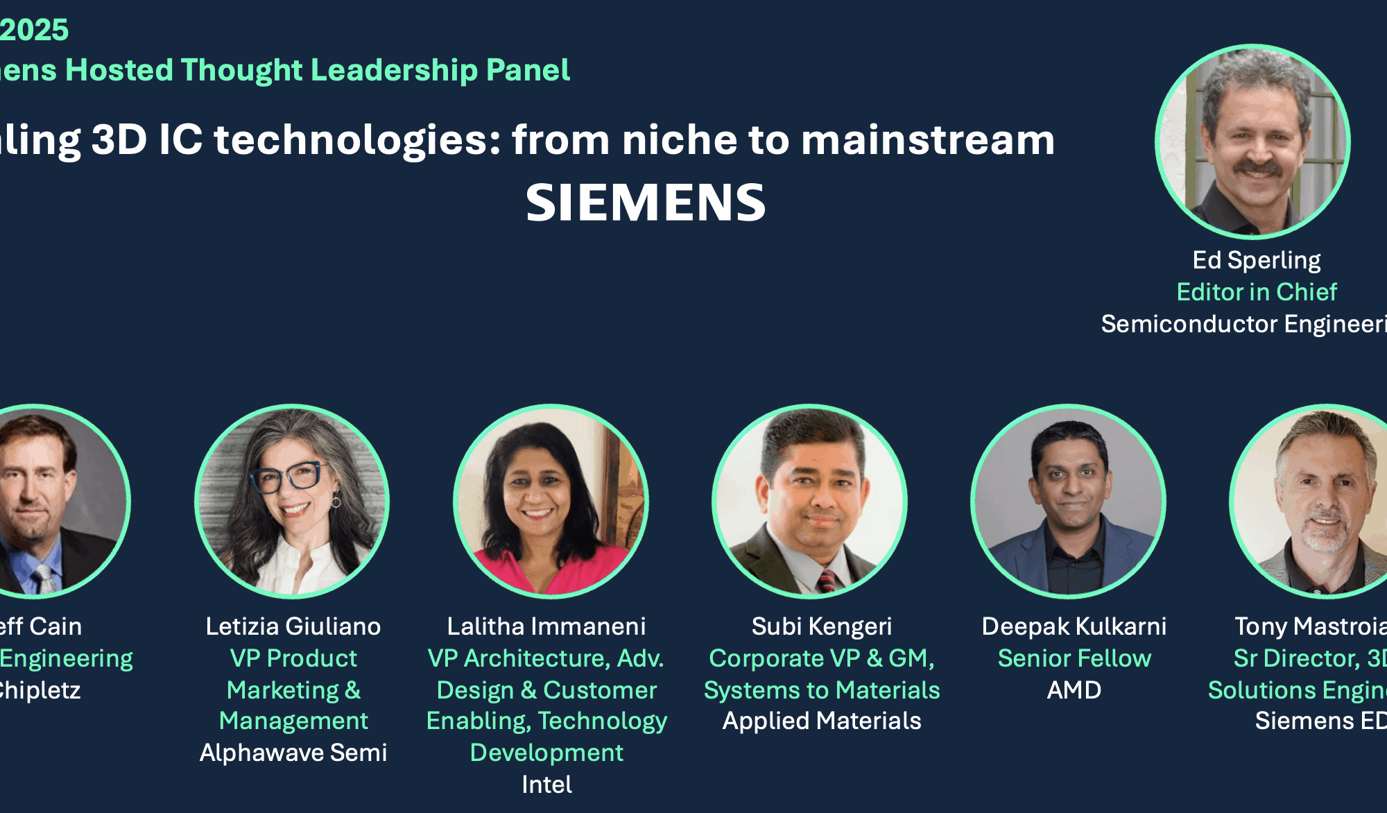
This is not hyperbole. Here’s a quick summary of who was on the stage. The lineup is also shown in the graphic above.
Ed Sperling, Editor in Chief, Semiconductor Engineering. Ed has either written for or been Editor in Chief for most of the mainstream technology publications for over 35 years. He was also a contributing editor for Forbes. Ed knows the hard questions and knows how to pose them.
Dr. Jeff Cain, VP of Engineering, Chipletz. Jeff represented the startup on the panel. He has been developing semiconductor solutions for 30 years, including half that time at Cisco. Chipletz is developing Smart Substrate™ products, an advanced packaging technology for chiplet-based design.
Letizia Giuliano, VP product marketing & management, Alphawave Semi. Letizia has been involved in marketing and engineering for advanced semiconductors for over 20 years at companies such as ST Microelectronics and Intel. She has been with Alphawave Semi for over five years.
Lalitha Immaneni, VP architecture, advanced design & customer enabling, technology development, Intel. Lalitha is an engineering leader with 30 years of experience in cross functional global engineering management, strategic planning/execution, and operations management.
Subi Kengeri, Corporate VP & GM, Systems to Materials, Applied Materials. Subi has over 30 years of experience in the design and manufacture of advanced semiconductor products. His career began at TI, and he has worked at companies such as Analog Devices, Virage Logic, TSMC, and GLOBALFOUNDRIES. He has been at Applied Materials for over five years.
Dr. Deepak Kulkarni, Senior Fellow, AMD. Deepak has worked in artificial intelligence, communication, and advanced packaging for 20 years. Dr. Kulkarni spent 15 years at Intel before joining AMD.
Tony Mastroianni, senior director, 3D IC Solutions Engineering, Siemens EDA. Tony has been developing advanced chip designs and advanced EDA tools for over four decades. I’ve known him for a long time, from the early days at RCA to later at eSilicon, where Tony was part of a pioneering team in multi-die design. He’s also worked at Silicon Design Labs, Silicon Compiler Systems, Mentor Graphics, and ASIC Alliance before joining Siemens EDA about five years ago.
Some Snippets of the Conversation
Here are some questions posed by Ed Sperling and summarized responses from the panelists.
From your broad vantage point, where do you see 3D IC trends taking off?
Tony Mastroianni: Hyperscalers have been doing this for some time. Automotive is starting to adopt the technology. Mil aero and defense are joining in as they really need this technology to advance the class of designs before them.
The current driver for 3D IC is AI data centers. A lot of those designs are driven by the hyperscalers and will never be sold commercially. Is this the start of a real market, of just a few customers who will drive massive demand?
Deepak Kulkarni: AI data center applications are driving early progress, but these programs are validating technologies that will see broad use in many designs if they are proven to be efficient and cost-effective. AMD 3D V-Cache is an example of this.
Lalitha Immaneni: We would like to see the ideal world of re-usable chiplets across various applications. This utopian concept of a chiplet marketplace is desirable, but there is still work to do in the ecosystem. Standards will be needed, things like performance specs with clear technology and product targets for example.
Many have said 3D IC is all about the interconnects, moving data from one area to another. Is this a growing market or is it still just a bunch of experiments?
Letizia Giuliano: To move away from a monolithic design style will require a lot of up-front planning on how interfaces will be done. Each interface requirement will need a dedicated solution. One configuration for all won’t work. Each channel interconnect will have unique requirements. Flexibility will help, but there must be dedicated, proven configurations. One must carefully manage power, area, and latency budgets. These efforts are underway and will be broadly valuable.
A lot of the new devices are looking at completely new materials. There are structural and thermal issues, with the possibility for things to go wrong. What are you hearing from your customers?
Subi Kengeri: To step back a bit, chiplet evolution has been driven by three key factors. Defect density drove the need for smaller dies, ease of design re-use in a proven technology was another driver and the ability to integrate heterogeneous functions in the best-fit technology was a third. We now need high levels of signal, power and thermal performance for this to all work. Applied Materials spends about $3.5 billion each year to address these challenges by validating new materials. We must stay ahead of the rest of the semiconductor industry.
Jeff Cain: What we do at Chipletz is work on next generation substrate technology. We want to go back to the OSAT model. That is, source multiple components and reliably package them for final delivery. We believe the technology to enable this will be ready in about a year. Our vision is to remove dependence on one supplier and make the process more predictable.
Tony Mastroianni: There is promising work on very large substrates. This could be a few years out, but it will enable massively large systems. Many technologies must come together to enable these designs. AI will play a key role. It’s not just a packaging challenge; it’s a system design challenge. The tools involved must work well together and this is an area Siemens EDA is focusing on. Managing the data and meta data is another focus area for us. This will be needed to enable AI solutions. And we’re working with the ecosystem to develop vendor neutral standards that will be needed as well.
In Summary
There were many more useful conversations during this one-hour event. I hope the snippets above give you a feeling for where the conversation went. I left the event with an upbeat outlook for the future of 3D IC design. Looking back, the companies on the panel are competitive with each other. The competition is still there, but the need to collaborate to pave the way to next generation technology was quite strong. This is new.
That attitude of “we all win” was refreshing and created an optimistic view of the future for me. All the companies on this panel are doing important and high-impact work to advance the cause. You can watch the entire event here. And you can learn more about what Siemens EDA is doing to advance 3D IC technologies here. And that’s how Siemens hosts a meeting of the minds at DAC.
Share this post via:


Comments
There are no comments yet.
You must register or log in to view/post comments.