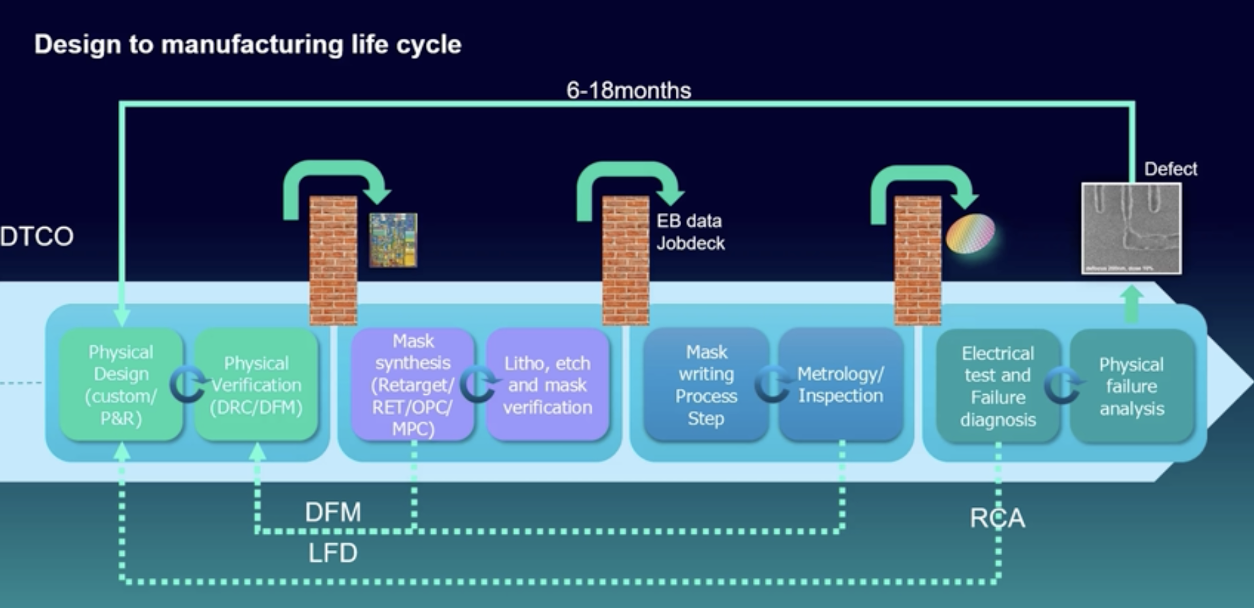
Preventing the propagation of systematic defects in today’s semiconductor design-to-fabrication process requires many validation, analysis and optimization steps. Tools involved in this process can include design rule checking (DRC), optical proximity correction (OPC) verification, mask writing and wafer printing metrology/inspection (to gauge the process), wafer printing metrology/inspection, and physical failure analysis to confirm failure diagnosis. The exchange of information and co-optimization between these steps is a complex process, with many feed-forward and feed-back loops. Communication is often hampered by “walls” between various parts of the process technology, slowing innovation. At the recent SPIE conference Siemens EDA presented a keynote address that proposed a series of approaches to break down these walls to improve the chip design to manufacturing process. Read on the see how Siemens aims to break down innovation barriers by extending design technology co-optimization.
About the Keynote
SPIE is the international society for optics and photonics. The organization dates back to 1955 and its conference has become a premier event for advanced design and manufacturing topics. At this year’s event, Siemens presented the keynote that is the topic of this post. There were many contributors to the presentation, including Le Hong, Fan Jiang, Yuansheng Ma, Srividya Jayaram, Joe Kwan, Siemens EDA (United States); Doohwan Kwak, Siemens EDA (Republic of Korea); Sankaranarayanan Paninjath Ayyappan, Siemens EDA (India). The title of the talk was Extending design technology co-optimization from technology launch to HVM.
The talk was part of a session on design technology co-optimization (DTCO). This concept isn’t new, but Siemens looked at its application across a broader scope of the process, from design to high-volume manufacturing (HVM). The ideas and results presented have significant implications. Let’s take a closer look.
What Was Presented
First, a look at the current state of DTCO usage across key parts of the ecosystem was presented. From a design perspective, many advanced fabless companies have a DFM team that is seeing the limits of a pattern-based approach. What is really needed is new technology to facilitate yield learning without foundry dependence.
The foundries are using brute-force pattern-based machine learning approaches, which are costly but not completely effective. They are also seeking efficient information mining of the massive manufacturing data they create. Equipment vendors and EDA vendors have been working closer together and are coming up with more efficient machine learning solutions.
Stepping back a bit, it was pointed out that there are walls between the design and manufacturing phases of the process. Fabless companies create the design, perform DRC and design for manufacturing (DFM), then they toss it over the wall to the OPC/RET team within the foundry or IDM. The design gets tasks such as OPC and verification done, and then the data is tossed over another wall for mask writing and metrology/inspection. The final wall is for fabrication. Here, electrical test and failure analysis will be done. By the time a root cause of failure is found, 6-18 months have passed. That’s a very long feedback loop. The graphic at the top of this post depicts this process.
DTCO attempts to break down the walls, but the methodologies available are incomplete. Traditional DTCO starts very early in process development. Starting with a scaling need, a standard cell is defined, and synthesis, place, and route are performed to come up with basic patterns and measure the performance and power. SRAM yielding is also done and that data loops back to the standard cell design.
What was presented at the SPIE keynote was a way to extend this co-optimization concept to the entire process from design to manufacturing. The approach involves enabling an easier flow of information from design all the way to the final process and physical analysis by creating an information channel.
While this sounds straight-forward, it is not. Many challenges were discussed with concrete approaches to mitigate the issues. For example, early designs can be created with layout synthetic generators to help calibrate the process to real design issues as the process is developed. This can alleviate many of the surprises currently faced with early process tapeouts.
Dealing with massive data volumes is another challenge. Using new sophisticated compression techniques, a 30X improvement is possible. This improves the data handling and analysis tasks quite a bit. A concept called explainable AI can help to find root causes of problems much faster. The ability to re-train AI models later in the manufacturing process without invalidating earlier results is another area for improvement. Also in the data analysis area are techniques to deal with “imbalanced data”. For example, there may be one hot spot found in 100,000,000 patterns.
Putting all this together can create a much more efficient end-to-end design flow, as shown in the figure below.

To Learn More
The impact of the approaches outlined in this keynote presentation is substantial. You can view the presentation and access a white paper on the process here. There’s a lot of useful information to be gained. And that’s how Siemens aims to break down innovation barriers by extending design technology co-optimization.
Share this post via:


Comments
There are no comments yet.
You must register or log in to view/post comments.