For more than 65 years, the IEEE International Electron Devices Meeting (IEDM) has been the world’s pre-eminent forum for reporting technological breakthroughs in the areas of semiconductor and electronic device technology, design, manufacturing, physics, and modeling. As I post this, the conference is underway in San Francisco and Intel is presenting a series of first-of-a-kind advances to extend Moore’s Law. The palette of innovations being presented at the conference creates a new path to vertical device scaling, opening the opportunity for a trillion transistors on a package by 2030. This is a story with several parts. Here are the details of how Intel previews new vertical transistor scaling innovation at IEDM.
The Impact
Everyone knows about the incredible exponential scaling delivered by Moore’s Law over the past 50 years or so. We’ve also seen the monolithic effects of Moore’s Law slowing of late. Multi-die design is now adding to the exponential density increases the industry has come to rely on. But that’s not the whole story. It turns out on-chip transistor density scaling is alive and well and is a key contributor to semiconductor industry health.
And Intel, the birthplace of Moore’s Law, is leading the way with innovation that fuels both monolithic and multi-die trends. In the area of advanced packaging to fuel multi-die design, you can read about Intel’s innovation with glass substrates here. The subject of this post is what Intel is doing to fuel the other trend – monolithic transistor scaling. This is a story of innovation in the Z-axis; how to stack devices on top of each other to deliver more in the same area.
It turns out there are two fundamental barriers to overcome here. First, how to stack CMOS devices to deliver reliable, high-performance characteristics. And second, how to get power to those devices without reducing reliability and performance. There are a series of presentations at IEDM this week that present several innovations that address these problems. Here are some details…
A Preview of Intel’s Announcements
I was fortunate to attend a pre-IEDM briefing where some of Intel’s advanced researchers previewed what was being presented at IEDM. What follows is a summary of their comments.

First to speak was Paul Fisher, Director of Chip Mesoscale Processing Components Research at Intel. Paul began with an introduction to the Components Research Group. He explained this organization is responsible for delivering revolutionary process and packaging technology options that advance Moore’s Law and enable Intel products and services. Some of the research that came from this group and found its way into commercial Intel products includes strained silicon, high-K metal gate, the FinFET transistor, Power Via technology and the RibbonFET. The list is much longer – quite impressive.
Another remarkable characteristic of this organization is the breadth of its worldwide collaboration. Beyond US government agencies, Paul explained the group also collaborates with consortia around the world such as Imec, Leti, Fraunhofer, and others in Asia. The group also directly sponsors university work and mentors other programs through organizations such as the Semiconductor Research Corporation (SRC). The group also works with the semiconductor ecosystem to ensure the equipment and processes needed for new developments are available.
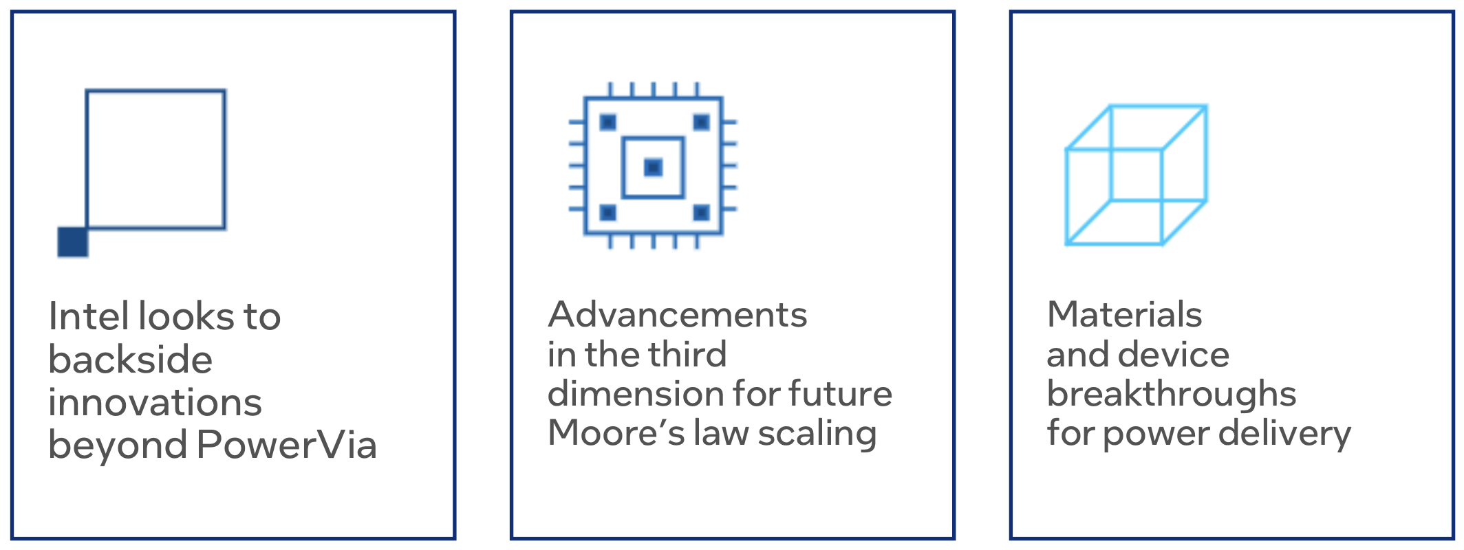
Paul then set the stage for the three briefings that followed. The first discussed innovations in backside power delivery. The second discussed three-dimensional transistor scaling and interconnect. And the third presented advances for on-chip power delivery using Gallium-Nitride (GaN). These three areas are summarized in the top graphic for this post.

Next to speak was Mauro J. Kobrinsky, Intel Fellow, Technology Development Director of Novel Interconnect Structures and Architectures. Mauro began by explaining that large, low resistance power routing competes with fine, low capacitance signal routing. The result is a compromise in density and performance. A significant advance that reduces this problem is back-side power delivery. Using this approach, power delivery routing can be done on the backside of the device, freeing critical front-side real estate for more optimal signal routing.
Mauro explained that Intel’s Power Via technology will move to production is 2024 and this will begin to open new options for back-side power delivery. Additional research will also be presented that takes back-side power delivery to a new level. This includes the development of back-side contacts to allow power to be delivered through the backside while signals are delivered through the front-side of the device.
Mauro also discussed critical enhancements for stacked device routing that are underway. Stacked devices present a unique set of challenges for both power and signal routing. In the signal area, new approaches for epi-epi and gate-gate connection must be developed and this is part of the research Mauro discussed.

After Mauro, Marko Radosavljevic, Principal Engineer at Intel discussed three-dimensional transistor scaling and interconnect. Essentially what comes after RibbonFET. Marko explained that initial device stacking results were presented by Intel at IEDM in 2021.
What will be presented at IEDM this year is the implementation of a vertically stacked NMOS and PMOS RibbonFET device configuration with Power Via and direct back-side device contacts with a poly pitch of 60nm. The resultant compact inverter exhibits excellent performance characteristics, paving the way for more widespread use of vertical device stacking.
The final speaker was Han Wui, Principal Engineer, Components Research at Intel. Han discussed new approaches to on-chip power delivery. He explained that Intel proposed the first MOS power driver in 2004. This device, often called DrMOS is now used in a wide variety of products.

Han went on to explain that Gallium Nitride, or GaN devices are popular today for high-voltage applications like the 200-volt devices in many laptop charging “bricks”. It turns out GaN exhibits far superior performance at lower voltages (48-volt and below) when compared to CMOS power devices.
At this year’s IEDM, Han explained that Intel will show the first implementation of a process that integrates CMOS devices with GaN power devices on a 300mm wafer. Dubbed DrGaN, Han explained that this technology will open new levels of performance and density for future designs by integrating CMOS drivers with highly efficient GaN power devices on the same wafer.
To Learn More
You can get a broader view of Intel’s device and process innovation here. And that’s how Intel previews new vertical transistor scaling innovation at IEDM.
Also Read:
Intel Ushers a New Era of Advanced Packaging with Glass Substrates
How Intel, Samsung and TSMC are Changing the World
Intel Enables the Multi-Die Revolution with Packaging Innovation
Share this post via:


Comments
3 Replies to “IEDM Buzz – Intel Previews New Vertical Transistor Scaling Innovation”
You must register or log in to view/post comments.