“Innovations for Next Generation Scaling”
The 2013 Forum today (Feb 5, 2013) started with a presentation by Dr. Gary Patton, VP, IBM Semiconductor Research & Development Center. Gary very clearly articulated the two irresolvable challenges the industry now faces:
- On chip interconnect
- Lithography
These two challenges connect very well with our recent blog IEDM 2012 – The Pivotal Point for Monolithic 3D IC. Gary showed both the exponential increase of RC which results from the dimensional scaling of copper below 100nm width and the high cost associated with double and quad patterning. In addition, he showed how the extreme scaling of the copper metallization creates reliability challenges such as fatal EM modes, and scaling of the insulator k breeds TDDB and strength issues. As a reminder, in the recent IEDM (Dec. 2012) short course, IBM presented the following slide indicating that interconnect now dominates device power!

L. Chang, D.J. Frank – IEDM 2012 Short Course – IBM Watson Research Center
Gary also presented a multi-decade past to future slide that resembles the one presented here below. The decade ending at the year 2000 was the good old days of easy scaling of planar transistor, which he called the gate oxide limit. Then the industry followed with a decade of “Material Innovation” that he called the planar device limit, and starting in 2010 is the beginning of the “3D Era” – 3D transistors and stacked devices.

Finally he shared with us his vision of 3D devices with three planes of devices:
- Logic Plane
- Memory Plane
- Photonic Plane
A vision we mutually share.
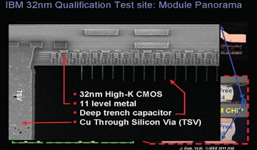
Now, here is my failure to understand. As a company who has been in the forefront of 3D and TSV research, IBM is well aware of the severe limitations of TSV as an alternative for vertical interconnect. The following cross-sectional picture by IBM, presented at the recent GSA Summit, clearly illustrates how large a TSV is in comparison to an interconnect via.

IBM Systems and Technology Group – GSA Silicon Summit 2012 (S.s lyer) – 2012 IBM Corporation
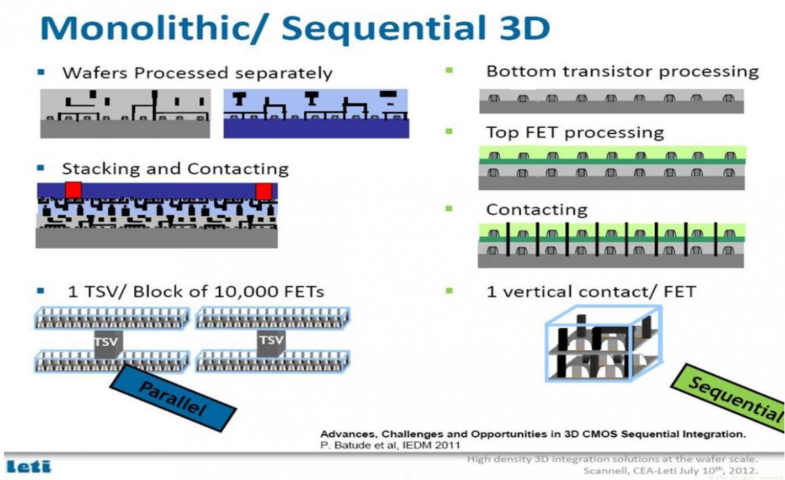
With TSVs of 5 micron diameters (and pitches of 15 micron due to keep out zones from stress issues) vs. vias of less than 50 nm, the ratio in vertical connectivity is 1:10,000 as illustrated in the following chart by Perinne Batude of CEA Leti.

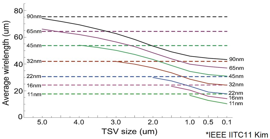
Clearly IBM technologists are well aware of the many research papers showing that TSVs, with their relatively huge size compared to all the other on-chip elements, diminish the performance or power benefits in folding designs to 3D. For example, the chart below was presented by Kim at the 2011 IEEE International Interconnect Technology Conference. The chart illustrates the performance benefits of folding a design twice (4 tiers of transistors) as dependent on the via size. At a via size of 5 microns there are actually no benefits, while at a via size of 0.1 micron the benefits are the equivalent of two nodes of dimension scaling!!!

So can someone please explain to me how come IBM is still talking about TSV as if it is the only representative of the “3D Era”???
And particularly now, when monolithic 3D is finally practical, and the NAND Flash memory vendors are adopting it across the board!?
Share this post via:


Musk’s Orbital Compute Vision: TERAFAB and the End of the Terrestrial Data Center