 AI is disruptive and transformative to many status quos. Its manifestation can be increasingly seen in many business transactions and various aspects of our lives. While machine learning (ML) and deep learning (DL) have acted as its catalysts on the software side, GPU and now ML/DL accelerators are spawning across the hardware space to provide performance leaps and growing capacity to the compute hungry AI data processing needs.

For the past few decades EDA has bridged the hardware and software space, transforming many electronic design challenges into solutions that became key enablers or drivers for its adopters to push the technology envelopes further. Being at the HW and SW technology crossroad, many EDA providers have embraced AI by either having their solutions augmented with ML assisted analytics or expanding its features to enable AI centric designs or applications.
AI Enablers and Challenges
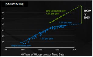 According to nVidia CEO Jen-Hsen Huang, the rise of AI had been enabled by two concurrent disrupting dynamics, i.e., how software development is done by means of deep learning and how computing is done through the more adoption of GPU as replacement to single-threaded, multi-core CPU, which is no longer scale nor satisfy the current increased computing needs.
Let’s consider these two factors further. First, the emergence of more complex DL algorithmic models such as CNN (convolutional neural network) and RNN (recurrent neural networks) has made AI based pattern recognition applications such as embedded vision and speech processings more pervasive.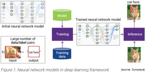
Training and inferencing steps, the two inherent and needed ML traits which mimic human cognitive development aspects, are subjected to different challenges. The former requires sufficient capacity and bandwidth, while the later demands latency optimization as it deals with irregular memory access issue.
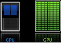
Secondly, on the hardware side, a CPU typically has a few to several dozens of processing units, some shared caches and control units. CPU is multi-purpose but has limited capacity. In contrast, a GPU employs numerous (hundreds to thousands) processing units with their own caches and control units, which are dedicated to perform specific works in parallel. This massive array of compute power and parallelism can absorb the workload presented by deep learning applications. GPU is well suited for training steps as it requires floating point engine while the inferencing portion may resort on a reduced accuracy or integer based data processor. Challenges to GPU architecture include the availability of adequate interconnect speed and bandwidth.
Aside from the above two factors, the advent of FinFET process technology has also played a major role in accommodating the integrations of the billions of devices into foundry allowed silicon die active area.
SoC and DesignWare Building Blocks for AI
Synopsys DesignWare® IP portfolio has been the foundation to chip design implementation for over two decades, containing technology- independent design IP solutions optimized for various cost factors (PPA). As DesignWare is at the epicenter of the ever evolving SoC implementation space, the list of DesignWare building block IP solutions has grown over the years, from a few number of compute primitives such as adders, multipliers to increasingly complex IP blocks such as microcontrollers, interface protocols (AMBA, USB, etc.) and eventually embedded microprocessors, interconnects and memories. Its integration also has been expanded to not only cover synthesis integration but also facilitate virtual prototyping and verification IP.
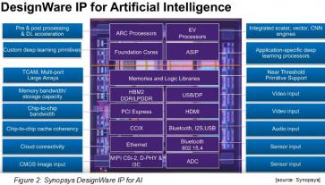
Designing SoCs targeted for AI related applications requires specialized processing, memory performance and real-time data connectivity. Recently, Synopsys upgraded its DesignWare IP portfolio for AI to also include these DL building blocks.
Specialized Processing
Specialized processors include embedded processors and tools for scalar, vector, and neural network processing. In order to handle AI algorithm efficiently, machine vision has relied on a heterogeneous pipelined processing with varying degree of data-centric parallelism.

As illustrated in figure 3, there are four stages associated with a visual data processing. The pre-processing step has the simplest data parallelism while the precise processing step has the most complex, requiring good matrix multiplication capabilities. Such unique processing needs can be served by Synopsys DesignWare ARC® processors. The DesignWare ARC EV6x processors integrate a high-performance scalar RISC core, a vector DSP, and a convolutional neural network (CNN) engine optimized for deep learning in embedded vision applications. The ARC HS4xD and EMxD processor families combine RISC and DSP processing capabilities to deliver an optimal PPA balance for AI applications.
Memory Performance
 AI models demand large memory footprint contributing to the overall silicon overhead as training neural networks requires massive memory space. Synopsys’ memory IP solutions include efficient architectures for different AI memory constraints such as bandwidth, capacity and cache coherency. The DesignWare DDR IP addresses capacity needed for data center AI SoCs.
Furthermore, despite the sustained accuracy promised by AI model compression through the pruning and quantification techniques, their adoption introduces irregular memory access and compute intensity peaks –both of which degrade the overall execution and system latency. This also drives the need for more heterogeneous memory architectures. DesignWare CCIX IP enables cache coherency with virtualized memory capabilities for AI heterogeneous compute and reduces latency in AI applications.
It is common that parallel matrix multiplication and increased size of DL models or coefficients necessitate the use of external memories and high bandwidth accesses. The DesignWare HBM2 IP addresses the bandwidth bottleneck while providing an optimized off-chip picojoules (pJ) per bit memory access. A comprehensive list of embedded memory compilers enabled for high density, low leakage, and high performance on-chip SRAMs options as well as TCAM and multi-port flavor are also available. Most of them are also ported to 7nm FinFET process node.
SoC Interfaces and Real-Time Data Connectivity
 Synopsys also provides reliable interface IP solutions needed between sensors. For example, real-time data connectivity between embedded imaging vision sensors and deep learning accelerator engine, normally done at the edge, is crucial as it is power sensitive. Synopsys offers a broad portfolio of high speed interface controllers and PHYs including HBM, HDMI, PCI Express, USB, MIPI, Ethernet, and SerDes to transfer data at high speeds, with minimal power and area.
Although DL SoCs have to deal with fluctuating energy metrics per operation due to massive data movement on and off chips, having both power management supported by memory IPs and the adoption of advanced FinFET process nodes such as 7nm, could provide an overall effective power handling.
As takeaways, designing for AI applications requires the understanding of not only the software or application intents but also the underlying data handling in order to deliver an accurate prediction within a reasonable compute time and resources. Having Synopsys’ silicon-proven DesignWare IP solutions as the building blocks will help accelerate the design realization while providing design teams with opportunities to explore an optimal fit to the more heterogeneous design architecture.
For more info on Synopsys DesignWare IPs please check HERE .
Share this post via:


Comments
There are no comments yet.
You must register or log in to view/post comments.