 One of the most interesting presentations that I went to was the last presentation at the Synopsys Custom Lunch (no, the lunch wasn’t custom, we all got the same, but the presentations were about custom design). Since the last presentation was by Synopsys themselves and not by a customer, it wouldn’t seem promising that it could be that interesting. But, as the saying goes, Synopsys “eats their own dogfood.” This is a phrase used in the software world (mostly) meaning that software companies use their own software.
But in a sense the presentation was by a customer. It was by Anwar Awad who heads up the IP design group at Synopsys. They use exclusively Synopsys tools for all their IP design. Since they are #2 in IP overall (perhaps depending on how you count Rambus) and #1 in interface IP, they are not someone easily ignored. Although Anwar talked a lot about the difficulty of designing IP for FinFET processes, I want to focus on the bigger picture.
Bringing up a modern process node such as 14/16nm to volume manufacturing depends on several things. First, obviously, the process needs to be ready and the fab needs to have been built (well, duh). But that is table stakes. Without other requirements being satisfied, the fab will sit empty losing $50/second. To run wafers, the designs need to have been done. And to do the designs, the EDA flows need to be in place.
But also the IP. Some advanced groups such as Qualcomm develop almost all their own IP and use very little 3[SUP]rd[/SUP] party IP. But most groups are not in a position to do that, they get IP from the IP companies. Often ARM for microprocessors and Synopsys for interface IP. Design groups cannot tapeout their designs until they have access to the IP. So Synopsys is on the critical path to volume ramp in leading edge fabs.
This has broken the logjam that used to exist with regards to PDK availability. If foundries want timely IP from Synopsys then they need to provide the IP group with timely PDKs. Like those old Visa ads where stores “don’t take American Express” the Synopsys IP group “doesn’t take Virtuoso PDKs” because they only use their own tools.
One thing that Anwar emphasized was that timely PDKs doesn’t mean waiting until every last number is available in its final form. That is much too late to start development of IP if it is to be available in time. Synopsys starts IP development with version 0.1 of the PDK, knowing that it will go through many revisions before they will get final numbers. Of course this results in a lot of redesign but the alternative is to be late.
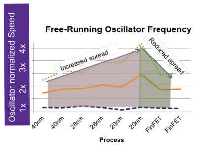
Synopsys have over 400 designers using their own tools for IP design, which in turns drives the tool development to delivering the factors necessary for success. IP design in FinFET processes is different from planar processes. So much of the silicon performance is dominated by layout parasitics that schematic simulation is largely irrelevant. Extracted layout is the only way to go. Of course this adds another wrinkle since now they have to do design with early DRC decks and adjust layout as the rules change.
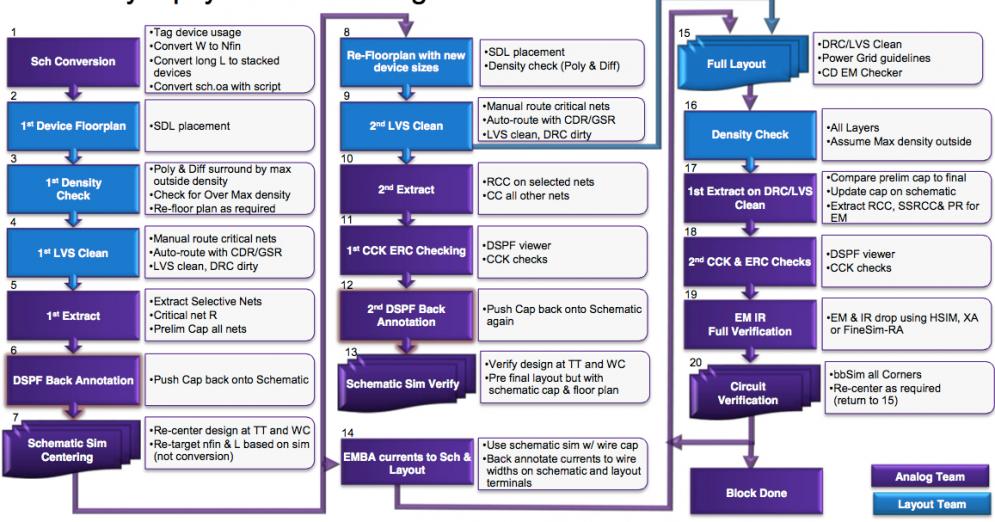
Anwar showed the details of the IP development tool flow (above, click to get a version large enough to read) and you can see just how many Synopsys tools are involved.
Here are his other golden rules for success dealing with moving decks, models, flavors, and project starts:
- Early LVS clean for extraction
- Use larger-than-min design rules where possible to minimize changes
- Leverage common blocks across IPs as much as possible – Single PLL team for example
- Run density checking after device placement
- Automation of running DRC with fill in place
- Single design/layout environment independent of the foundry
- Layout layers are common across all foundries to improve layout efficiency when moving from process to process
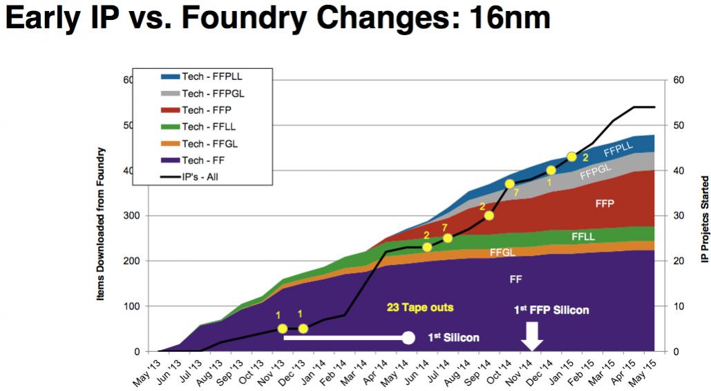
The diagram above shows the process for 16nm, showing when they started, when new projects were started and so on. This resulted in a lot of testchips for both the various flavors of TSMC and Samsung (which is also GF). The portfolio was USB2, USB3, DDR4, PCIe2, PCIe3, HDMI, DPHY, 10G KR, 16G.
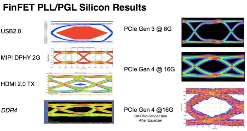
Although a lot can be done in simulation, ultimately there is no substitute for looking at the “eye diagrams” from measurements of real silicon running at speed (see above). This is especially so for a new process with a new feature such as FinFETs, and especially early in the design cycle when everyone knows that the PDKs are not final, the design rules will change.
In total they ran over 30 test chips. Presumably most were on MPW shuttles but even so that is a major investment (I don’t know what the financial arrangements were but I doubt Synopsys paid retail).
Synopsys Custom Design page is here
Wikipedia page on eating your own dogfood (really) is here
Share this post via:


Comments
There are no comments yet.
You must register or log in to view/post comments.