
The first article in this series examined how feasibility exploration enables architects to evaluate multi-die system configurations while minimizing early design risk. Once architectural decisions are validated, designers must translate conceptual connectivity requirements into physical interconnect infrastructure. Bump and TSV planning represents one of the most critical steps in bridging architectural intent with physical implementation.
Multi-die designs rely heavily on dense, high-performance interconnect structures to enable communication between chiplets, interposers, and package substrates. As multi-die systems continue to scale in complexity and signal density, traditional manual interconnect planning approaches are no longer sufficient. This article explores the methodologies and automation strategies that enable scalable bump and TSV planning. The final article in this series will discuss automated routing solutions that implement high-speed signal connectivity across these interconnect structures.
Why Bump and TSV Planning Is Critical
Bumps and TSVs form the electrical and mechanical backbone of multi-die systems. Microbumps and hybrid bonding pads facilitate horizontal connectivity between adjacent dies, while TSVs enable vertical communication between stacked dies and packaging layers. These interconnect elements allow multi-die architectures to achieve extremely high bandwidth and low latency communication.
As advanced packaging technologies reduce interconnect pitch, modern multi-die systems may include millions of individual connections. Because these interconnect structures influence routing feasibility, signal integrity, and power delivery efficiency, their planning must occur early in the design process. Poor interconnect planning can create routing congestion, degrade performance, and increase implementation complexity.
The Limitations of Manual Planning
Historically, designers relied on spreadsheet-based or graphical planning methods to define bump layouts. While these approaches were adequate for single-die flip-chip designs with limited connectivity, they cannot scale to modern multi-die systems. Manual planning increases the likelihood of connectivity mismatches between dies and introduces challenges when design changes occur during development.
Even minor modifications to bump placement can affect routing feasibility, interposer layout, and die placement. Coordinating such changes across multiple design teams becomes increasingly difficult as system complexity grows, making automation essential for maintaining design consistency and productivity.
Automated Bump Planning Methodologies
Modern multi-die design tools provide automated bump planning capabilities that allow designers to generate, place, and assign interconnect structures efficiently. By integrating bump planning into early design exploration and prototyping stages, designers can optimize multi-die floorplans and improve routing quality. Automated workflows support multiple input formats and allow designers to reuse or adapt existing bump maps across different designs and technologies.
Region-Based Bump Planning
To manage the scale and complexity of bump placement, designers often organize bumps into functional regions associated with specific interfaces or subsystems. Region-based planning allows designers to define placement patterns using parameters such as pitch, spacing, and bump geometry. These regions dynamically adjust as design constraints evolve, ensuring consistent placement and rule compliance throughout the design process.

Signal Assignment and Hierarchical Integration
After bump placement is established, designers must assign signals and power connections to individual interconnect structures. Automated assignment algorithms can optimize routability and wirelength across the entire multi-die system, rather than focusing solely on individual dies. Hierarchical planning capabilities further improve productivity by allowing bump structures to propagate between IP blocks and top-level die implementations, enabling efficient reuse and consistency.
Automatic Bump Mirroring and Alignment
Precise alignment between contacting dies is essential for ensuring electrical continuity and manufacturability. Automated mirroring techniques replicate bump layouts across adjacent dies while accounting for orientation and placement changes. This approach significantly reduces alignment errors and ensures that interconnect structures remain synchronized throughout design iterations.
Engineering Change Management (ECO) and Design Rule Checking
Bump planning is inherently iterative and requires robust engineering change management capabilities. Integrated visualization and reporting tools enable designers to track modifications and maintain synchronization across multiple dies and packaging layers. Multi-die-aware design rule checking ensures connectivity correctness, alignment accuracy, and compliance with logical and physical constraints, reducing the risk of costly late-stage errors.
Bump ECO Graphical Visualization and Spreadsheet-like Table

TSV Planning Considerations
TSVs introduce additional design constraints due to their size, mechanical stress impact, and area overhead. Designers must carefully position TSVs to minimize their effect on device placement and timing performance. TSV planning is often performed concurrently with bump planning to align vertical and horizontal connectivity structures and reduce routing complexity.
Synopsys 3DIC Compiler Platform for Building the Interconnect Foundation
Bump and TSV planning for a multi-die design is a critical, but tedious, time-consuming, iterative, and error prone step faced with multiple challenges. Creating optimal, DRC-correct bump maps and die-to-die connectivity plans for millions of bumps over multiple dies involving multiple designers is complex and critical to meet PPA targets and design schedules. Synopsys’ unified 3DIC exploration-to-signoff platform, meets those challenges with powerful bump planning, visualization, and analysis capabilities, increasing design engineer productivity and drastically cutting design time.
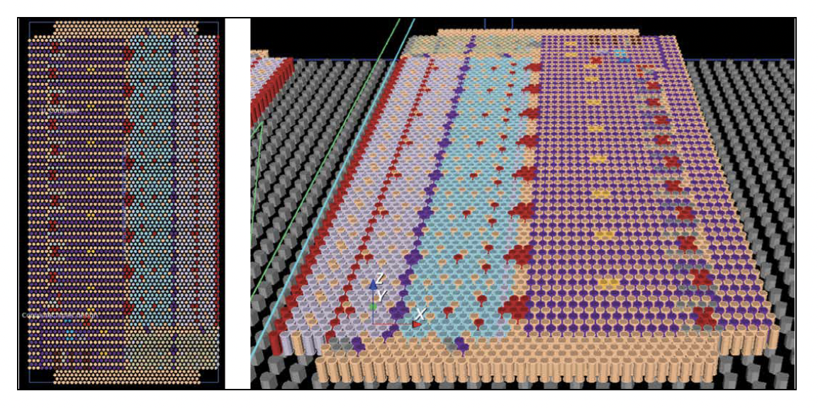
UCIe signal color-coded bump plan in 2D and 3D, as created in 3DIC Compiler platform

Learn more by accessing the whitepaper from here.
Establishing the Routing Framework
Effective bump and TSV planning creates the physical connectivity infrastructure required for high-speed signal routing. With interconnect structures defined and aligned across dies, designers can focus on implementing dense, high-performance routing for advanced chiplet interfaces. The final article in this series will explore how automated routing technologies enable scalable implementation of high-speed multi-die interconnects.
Also Read:
How Customized Foundation IP Is Redefining Power Efficiency and Semiconductor ROI
Designing the Future: AI-Driven Multi-Die Innovation in the Era of Agentic Engineering
Hardware is the Center of the Universe (Again)
Share this post via:


Comments
There are no comments yet.
You must register or log in to view/post comments.