
The semiconductor industry is entering a new era in system design. As traditional monolithic scaling approaches its economic and physical limits, multi-die architectures are emerging as a primary pathway for delivering continued improvements in performance, power efficiency, and integration density. By distributing system functionality across multiple dies or chiplets and integrating them within advanced packaging technologies, designers can create highly optimized heterogeneous systems tailored for demanding applications such as artificial intelligence, high-performance computing, and advanced automotive platforms.
However, the flexibility offered by multi-die architectures introduces a significant increase in design complexity. Unlike monolithic devices, where most interactions occur within a single silicon environment, multi-die systems introduce new dependencies across packaging technologies, power delivery networks, and interconnect strategies. Decisions made during the earliest stages of system architecture can have profound consequences on manufacturability, reliability, and performance. SemiWiki will be publishing a series of articles based on whitepapers released by Synopsys on the topic of multi-die systems.
This article, the first in a three-part series, examines the critical role of feasibility exploration in evaluating multi-die design architectures. Subsequent articles will explore how bump and Through-Silicon-Via (TSV) planning, followed by automated high-speed routing methodologies, translate architectural concepts into successful implementation.
The Growing Complexity of Multi-Die Design
Multi-die system integration requires designers to consider a broader and more interconnected set of constraints than ever before. System architects must simultaneously evaluate die placement and orientation, packaging configurations, interconnect density, and power delivery topology, while also accounting for thermal management strategies. Each design decision introduces ripple effects across the system, influencing both electrical and physical behavior.
Three interrelated performance metrics dominate early multi-die architectural evaluation. Power integrity, often measured through IR drop, directly affects functional reliability and timing margins. Electromigration introduces long-term reliability risks that can compromise device lifetime. Thermal performance determines whether the system can operate within safe temperature limits under peak workloads. In multi-die environments, these challenges become significantly more difficult to model accurately due to the interaction of multiple materials, stacked geometries, and distributed power and signal paths.
Why Early Feasibility Exploration Is Essential
Traditional design methodologies frequently relied on detailed physical implementation and signoff-level analysis to validate power, thermal, and reliability behavior. While highly accurate, these approaches are impractical during early architectural development because they require complete design data and extensive runtime. Feasibility exploration addresses this limitation by enabling designers to analyze architectural options using simplified but representative models.
Through feasibility workflows, designers can evaluate alternative floorplans, connectivity structures, and power distribution strategies without requiring full process design kits or finalized physical layouts. This abstraction dramatically accelerates iteration cycles, allowing teams to explore a broader design space and identify architectural weaknesses early in development. Early identification of issues such as excessive IR drop or thermal hotspots helps prevent costly redesign efforts later in the project lifecycle.
Feasibility vs. Prototyping: Understanding the Difference
Multi-die development typically progresses through two closely related but distinct exploration stages. The feasibility stage focuses on rapid architectural evaluation using abstract models and simplified floorplans. During this phase, designers assess whether proposed multi-die configurations can meet performance, power, and thermal goals without committing to detailed implementation.
Prototyping follows feasibility exploration and introduces technology-specific data and realistic physical structures. At this stage, interconnect models, packaging details, and implementation constraints become more accurate, providing a bridge between architectural exploration and production-ready design. Feasibility exploration therefore serves as the foundation upon which prototyping and detailed implementation are built.

Modeling Techniques That Enable Rapid Exploration
Successful feasibility exploration depends on modeling techniques that balance speed with predictive accuracy. One widely used approach involves pixel-based modeling of the power delivery network. By dividing the power distribution network (PDN) into regularly spaced elements with defined resistance characteristics across multiple dimensions, designers can efficiently evaluate voltage distribution and electromigration behavior across dies and packaging structures.
![]()
Simplified bump and TSV models also play a crucial role in early exploration. Rather than relying on foundry-specific implementations, designers can define key interconnect characteristics such as size, placement, and resistance. These models provide sufficient accuracy to evaluate connectivity density and power distribution behavior while maintaining rapid simulation turnaround times.
Thermal modeling further complements feasibility exploration by enabling designers to define material properties, thermal conductivity boundaries, and cooling strategies. These models allow engineers to quickly assess temperature distribution across complex multi-die stacks and packaging configurations.
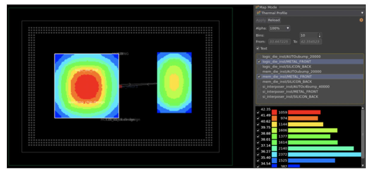
Visualization: Turning Analysis into Insight
One of the most valuable aspects of feasibility exploration is the ability to visualize analysis results. Graphical heat maps and power integrity plots provide immediate insight into system behavior, allowing designers to identify high-risk regions and refine architectural choices quickly. Visualization enhances collaboration across design teams and supports data-driven decision-making throughout early development stages.

Synopsys 3DIC Compiler Platform-Driven Feasibility Exploration
Unified multi-die design platforms such as the Synopsys 3DIC compiler platform have significantly improved the efficiency of feasibility exploration by integrating modeling, analysis, and visualization capabilities within a single environment.
The Synopsys 3DIC Compiler platform offers fast, flexible, integrated feasibility and prototyping capabilities to quickly and efficiently create, visualize, and analyze prototype designs. Through fast, simple, straightforward power, PDN, and thermal UI-based models, no foundry process design kit (PDK) or technology data is required to create the prototype designs. Built-in IR drop, electromigration, and thermal analysis technologies designed for fast feasibility exploration allow designers to iterate on possible architectures quickly and easily.
Learn more by accessing the whitepaper from here.
Setting the Stage for Interconnect Planning
Feasibility exploration establishes the architectural blueprint for multi-die implementation by validating die placement, power delivery strategies, and connectivity requirements. Once these architectural parameters are defined, designers must translate them into detailed interconnect structures. The next article in this series will examine how bump and TSV planning provide the physical foundation for scalable multi-die connectivity and prepares designs for implementation and routing.
Also Read:
How Customized Foundation IP Is Redefining Power Efficiency and Semiconductor ROI
Designing the Future: AI-Driven Multi-Die Innovation in the Era of Agentic Engineering
Hardware is the Center of the Universe (Again)
Share this post via:


Comments
There are no comments yet.
You must register or log in to view/post comments.