Harish Aepalais part of the Design Closure Methodology group at LSIand he recently talked about his ASIC handoff experience in a webinar. Harish works with logic and physical synthesis, timing constraints, RTL analysis and formal verification.
One challenge with ASIC handoff has been getting through design closure with the fewest iterations so that the physical design still meets timing, power and area budgets. To reduce these iterations Synopsysengineered the Design Compiler Graphical tool to offer an approach with a better starting point for faster physical implementation. LSI has successfully used Design Compiler Graphical in their ASIC handoff methodology.
Design Trends
SoC designers are creating systems with deep logic levels in order to reduce latency, the RTL is often not optimized for hierarchical design because of legacy re-use, there’s an explosion in the number of hierarchical blocks, and the data bus widths have become even wider. A typical SoC design at LSI can be characterized in the following table:
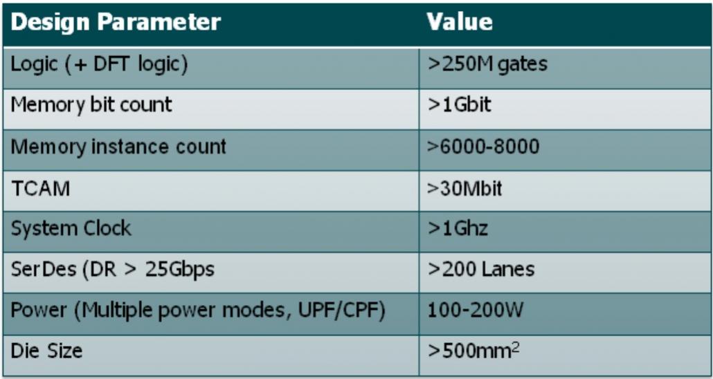
The QoR (Quality of Results) for physical implementation are challenged by these design trends.
Traditional Design Flow
For simple SoC designs the following traditional flow shows how a customer runs their RTL code through logic synthesis and hands it off to LSI for floor planning. The customer then runs physical synthesis until design closure is reached. Finally, LSI adds the test logic and completes place and route.
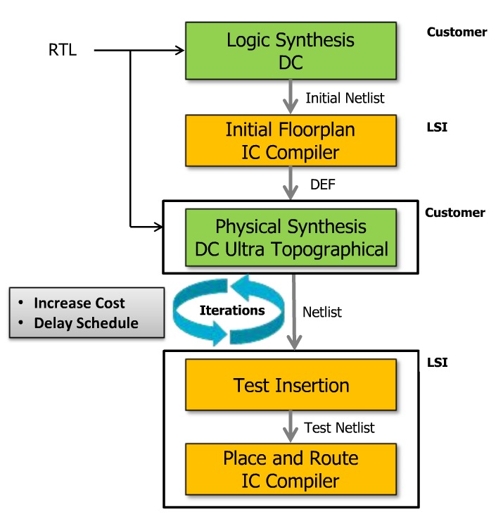
At each hand-off phase there are checks run to ensure compliance.
As SoC size and complexity increase the traditional design flow starts to break down.
LSI Recommended Flow
Leading edge SoC designs are better handled with an LSI recommended flow where the customer uses Design Compiler Graphical instead of the Design Compiler Topographical tool:
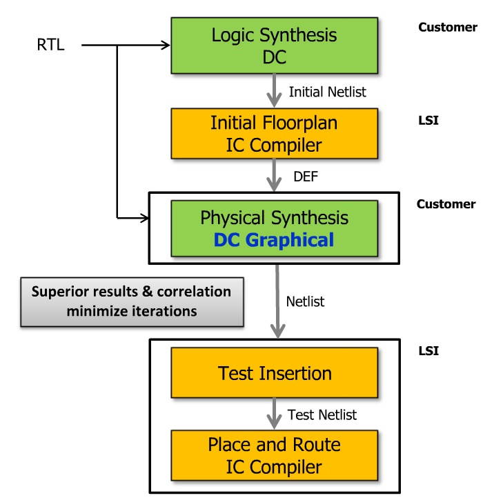
Timing, area, power and congestions issues are handled better in this flow with DC Graphical.
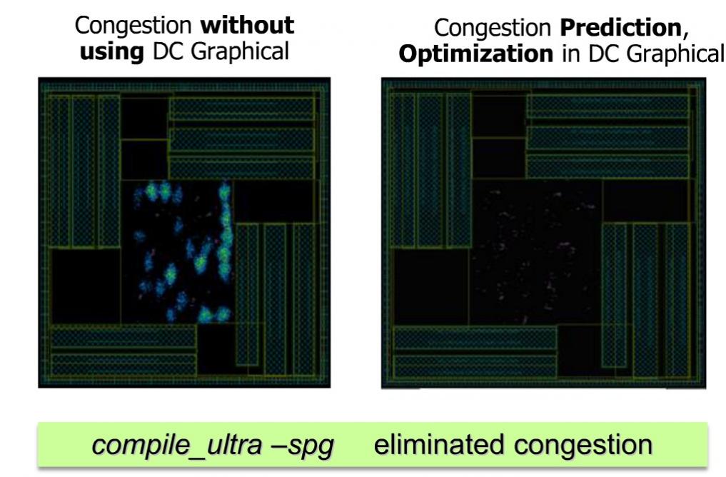
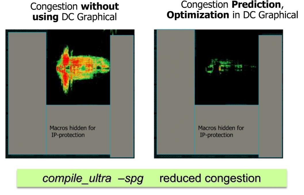
One LSI customer started using DC Topographical however during floor planning there were large multiplexors that clogged the routing congestion to an extent that the area requirement couldn’t be met. Switching to DC Graphical with congestion-related options created a higher QoR netlist that could meet the area requirement:
- Design Compiler directives
- set_ignored_layer
- set_congestion_options
- DC Graphical
- compile_ultra -spg
Results
Here’s the before and after congestion comparison for this 28nm design:
Another customer example used 40nm technology and the congestion was greatly reduced by using DC Graphical:
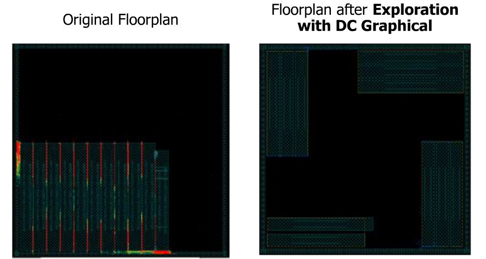
A third customer example shows how using DC Graphical allowed the customer of a 28nm SoC to modify their own floor plan to eliminate congestion overflow, eliminate iterations with LSI, and save one to two weeks in their schedule:
Timing as measured by Worst Negative Slack (WNS) and Total Negative Slack (TNS) can be compared between the traditional synthesis and DC Graphical approaches as shown below for a 28nm customer design:
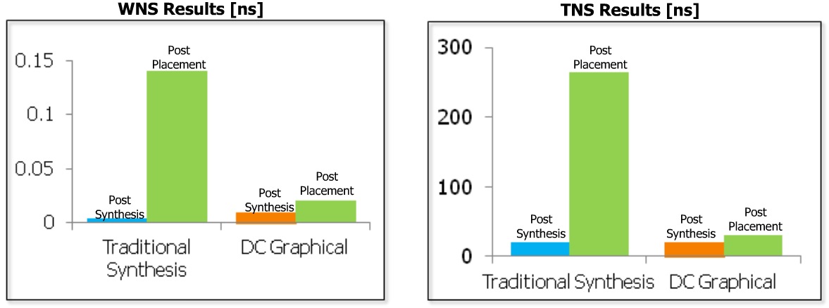
The Timing QoR are much better (smaller) with the DC Graphical approach for this design, plus the timing estimates were within 4% of post-placement results.
Summary
RTL designers can experience fewer design closure iterations and achieve better QoR by using DC Graphical. Comparison results from LSI show improvements in reducing congestion, shortened project schedules, lower area and reduced power.
lang: en_US
Share this post via:


Comments
0 Replies to “An ASIC Design Flow at LSI”
You must register or log in to view/post comments.