Bruce Caryl is a Product Specialist with Siemens EDA
The most common way to evaluate a power distribution network is to look at its impedance over the effective frequency range. A lower impedance will produce less noise when transient current is demanded by the IC output buffers. However, this transient current needs to be provided at the same time for each transition or jitter will be produced that will limit the maximum operating speed of the interface.
While not typically evaluated in PDN design, jitter can have a significant effect on the timing margins on single-ended nets found in interfaces such as double data rate (DDR) memory, limiting the maximum operating speed.
Jitter provides a metric for evaluating the quality of a PDN, since reducing it can improve the performance of a data-driven interface. . In this article we describe a simulation methodology to automatically measure the jitter caused by a PDN and use the results to evaluate the quality and effectiveness of the PDN decoupling.
The first step in measuring the jitter induced by a PDN is to create a good electrical model of the PDN that captures all its electrical characteristics, such as the frequency response of the decoupling capacitors, the mounting inductance of the ICs, and the spreading inductance of the planes. This can be done with a 3D electro-magnetic field solver, which is a hybrid of a full-wave solver, with simplifications to support a large power network structure. This type of model is often an S-parameter model with ports at the IC of interest and at the VRM connection.
The PDN model is then placed in a schematic and connected to a VRM model at the input and a driver current model as a load. The VRM model should be a simplified representation of the output impedance of the VRM, covering a range of frequencies below where the main decoupling capacitors are effective. The driver current model produces a linearly increasing current with time. The current waveform is based on a pseudo-random bit sequence so that a variety of frequencies are covered.
Finally, we need to measure the jitter produced by the varying driver current. We will use the VHDL-AMS behavioral language to create a model that can measure the jitter between the driver current waveform and the resulting waveform produced at the output of the PDN. The model will keep track of the largest jitter, as well as the generated voltage noise, and report that in the output waveforms.
Interpreting PDN Performance
Once the testbench has been created, it is easy to substitute various PDN models and then quickly determine how much jitter each PDN implementation introduces. You can add or remove decoupling capacitors and see what the impact would be. You can also experiment with different capacitor values to see which combination is best.
One of the challenges with setting up the simulation is determining what the data rate and edge rate should be when the stimulus is directly connected to the PDN. In the real design, the IC has additional decoupling due to the package and die capacitance. We could add that to our model, but that information is often hard to come by. As a compromise, we will assume that for our DDR4 power net example (1.2 V), the edge rate is slowed to 200 ps by the package and die. For the data rate we will use 4 ns per UI, which corresponds to a 125 MHz Nyquist frequency. This is near the upper frequency limit in which we expect the PDN to be effective. The PRBS stimulus will then produce 4 ns transitions and many sub-harmonics, stimulating the PDN at a variety of frequencies.
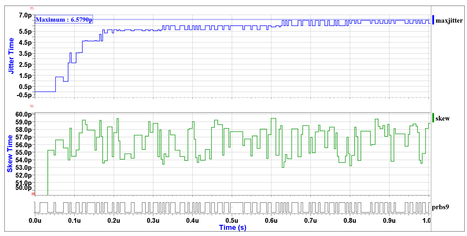
Figure 1 shows the maximum jitter (maxJitter), the skew per edge transition, and the PRBS9 data pattern. After about 1.0 µs, the jitter does not increase significantly for the applied data pattern. The maximum jitter is shown to be about 6.6 ps for both the rising and falling edges.

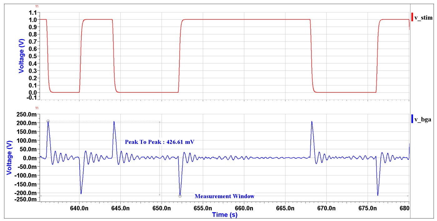
We can also display the noise generated at the BGA pins (blue) caused by the stimulus (red), shown in Figure 2.

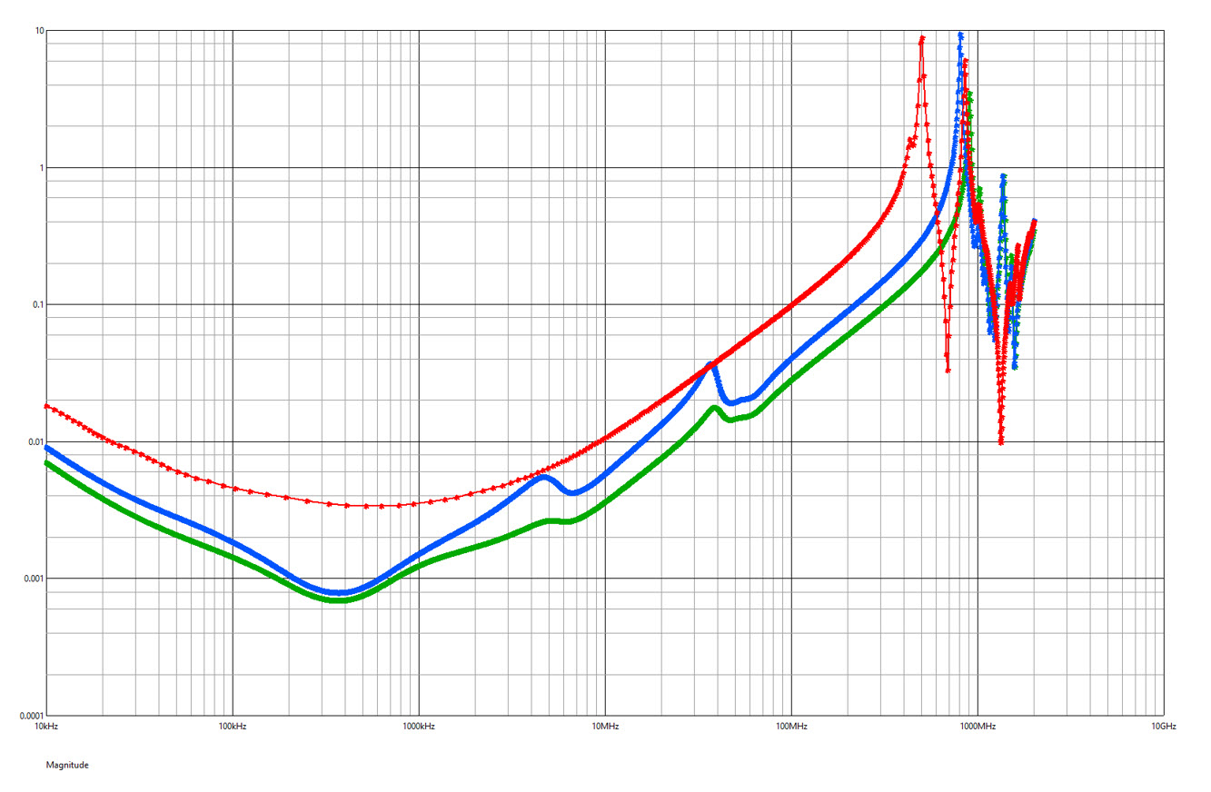
We can now use this technique to compare multiple PDNs to see how they perform. First, we extract the frequency domain models for three decoupling configurations and look at the Z-parameter (impedance versus frequency) plots, as shown in Figure 3. The green plot is the actual decoupling used on the 0.85 V power in a working design. The blue plot is the impedance with all the 100 µF and 4.7 µF caps removed, and the red plot is the optimized impedance profile, which has a higher impedance magnitude but a smoother and flatter impedance profile.

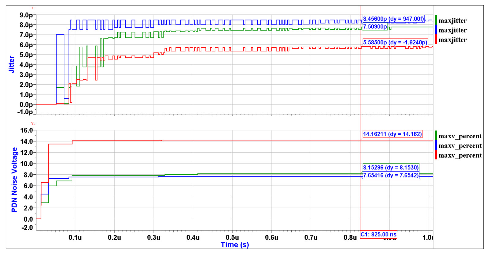
In Figure 4, we compare the jitter produced by the three different PDNs, and we see that the lowest jitter (5.6 ps) comes from the optimized PDN (red), which has the flattest impedance curve. The next lowest jitter (7.5 ps) is from the actual PDN as designed (green). When we remove some capacitors but keep a similar profile, the impedance and the jitter (8.5 ps) both go up (blue).
Looking at the noise amplitude as a percentage of the signal (maxv_percent), we see a direct correlation between the impedance and the noise induced by the PDN, as expected. If we look at impedance as the only quality metric for the PDN, we might conclude that the lowest impedance PDN has the best performance. However, we see that while the noise amplitude is lower, the jitter is higher.
The PDN was optimized by selecting capacitors that just met a flat impedance profile. This flatter profile also has a more consistent phase shift over the frequency range, so the edges for all data transitions tend to be more aligned and thus produce less jitter.
You may have wondered whether a flat impedance profile is better than a so-called “deep V” profile, where most of the caps have the same value. In this case, it appears that the flatter profile produces better jitter performance, which may be an important consideration for output data switching signals.

So, the next time you are thinking about how robust your PDN is, consider how well it can supply current at the right time across all frequencies. PDN induced jitter is another factor that can limit a high-speed design’s performance.
Please download the full white paper, Evaluating a PDN based on jitter, to learn more about this methodology and to see how adding capacitors can sometimes create even more jitter.
Bruce Caryl is a Product Specialist focused on board analysis products, including signal and power integrity, and mixed signal analysis. Prior to this role, he worked in product and technical marketing, consulting, and applications engineering. Bruce has authored several white papers on analysis techniques based on the needs of his customers. He began his career as a design engineer where he did ASIC and board design.
Also Read:
DAC News – A New Era of Electronic Design Begins with Siemens EDA AI
Siemens EDA Outlines Strategic Direction for an AI-Powered, Software-Defined, Silicon-Enabled Future
Share this post via:


Comments
There are no comments yet.
You must register or log in to view/post comments.