Often designers are amazed at the diversity of requirements fabricators and manufacturers have for metal filled areas in advanced package designs. Package fabricators and manufacturers do not like solid metal planes or large metal areas. Their strict metal fill requirements address two main issues. The dielectric and metal layers can be very thin, 15 µm or less, and during the build-up and RDL process they can suffer from areas of delamination due to trapped pockets of gas. Think of it being like adding a screen protector to your smartphone and how hard it is to get the air bubbles out. Also, uneven conductor densities on the same layer or across layer pairs can cause warpage in the package and/or the wafer.
The combination of these issues makes the designer’s job of meeting the manufacturing rules a challenge. Further, the diversity of substrate technologies from numerous vendors means there’s no one-size-fits-all solution. In this article, we will walk through three methodologies that are commonly utilized on advanced package designs to achieve foundry/OSAT requirements for metal areas and planes:
- Dynamic hatched filled metal areas
By far the easiest and fastest methodology. Some additional steps may be needed based on the density requirements. - Outgassing voids in metal areas
A post process solution that can be customized for about any situation. - Dummy metal fill
This is the way most silicon designs handle low density areas. Typically used for silicon interposer designs.
Dynamic hatched filled metal areas
One of the simplest ways to solve both outgassing and metal fill coverage is to use dynamic hatched fill. When adding square or diagonal hatch, the package design tool should tell you what the base density will be across the plane, which makes hitting your target density fairly simple.

You will need to make sure to fill any incomplete or partial hatches to prevent acute angle issues, and you should also offset the hatch on adjacent layers to prevent EMI and signal integrity issues. By setting these up in the beginning of the project, you save time over doing it at the last minute just before or during tape-out. Most manufacturers and fabricators have manufacturing sign off design rules that need to be met before manufacturing can begin. These design rules check for manufacturing and yield issues, like spacing, and problem layout items, like acute angles, density, and fill. When violations are found, designers can save time finding and fixing them by cross-probing from the design rule checking tool to the layout tool, if that capability is supported.

Figure 1. 30 µm void, 40 µm pitch, 43% fill
In some technologies the base hatch can be amended to add other features required for a specific vendor.

Figure 2. HDFOWLP with pad voids and additional plane voids
Dedicated outgassing voids
It is common to see designers utilize standalone outgassing voids. Unlike the dynamic hatched fill, this is a post process. Designers use outgassing voids to get void shapes—like circles, rectangles, oblongs, octagons, or hexagons—or to stagger the voids. Once you find your formula, the process is predictable and very easy to update for layout changes. Using a density-aware, multi-pass outgassing routine enables designers to work on signal integrity and power integrity issues while simultaneously considering the manufacturing process requirements — resulting in significant time savings.
Metal balancing can be a density per layer or a layer pair target. Some manufacturers also utilize sub-layer blocks (125 µm–250 µm windows of density), like walking blocks or adjacent blocks.
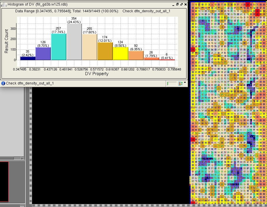
Figure 3. 125 µm density sub-block regions
Whatever the rules, make sure the adjacent layer voids are offset and keep the voids from going over any differential signal routing. Differential signals or pairs can have issues if the voids are unevenly dispersed on the adjacent layers over the pair. You may also see clearance rules from the void to a micro-via/polyamide opening or to a trace.
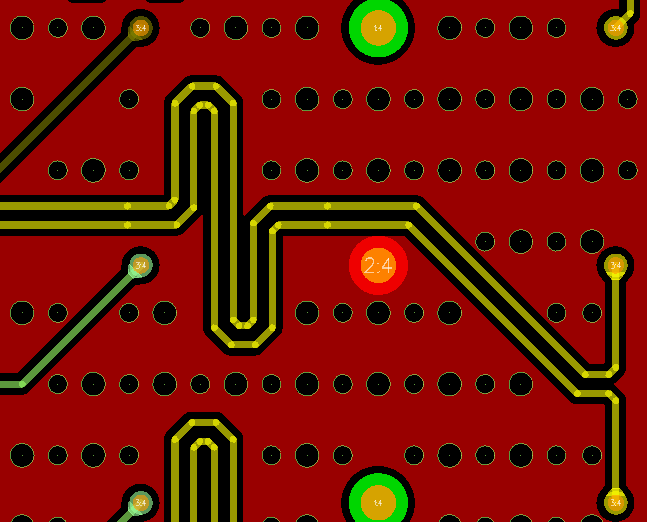
Figure 4. Multi-pass density aware voids
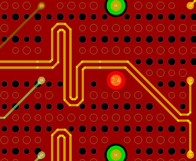
Figure 5. Adjacent layer void clearance
In high-speed designs or designs with high current draw, designers utilize automation guided manual void placement. This helps users to meet the manufacturing requirements while being fully aware of where each void is getting placed. 5G packages are a perfect use case for this method and is recommended over the shotgun approach of the fully automated methods where manual cleanup of unwanted voids is too time consuming.
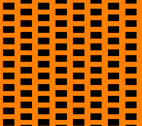
Figure 6. Staggered rectangle voids to differential pairs
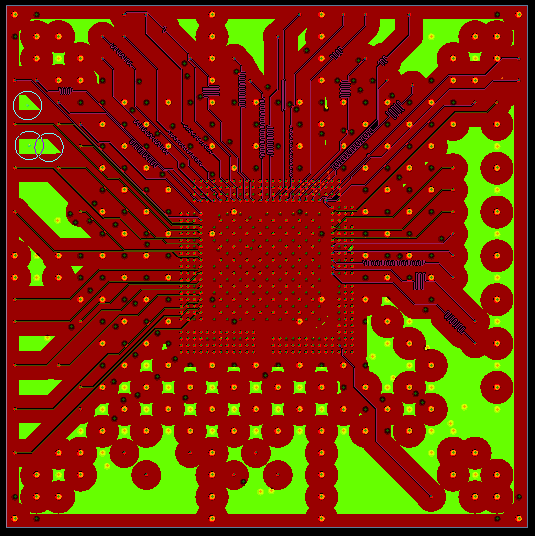
Figure 7. Degassing void analysis identifies areas requiring void insertion
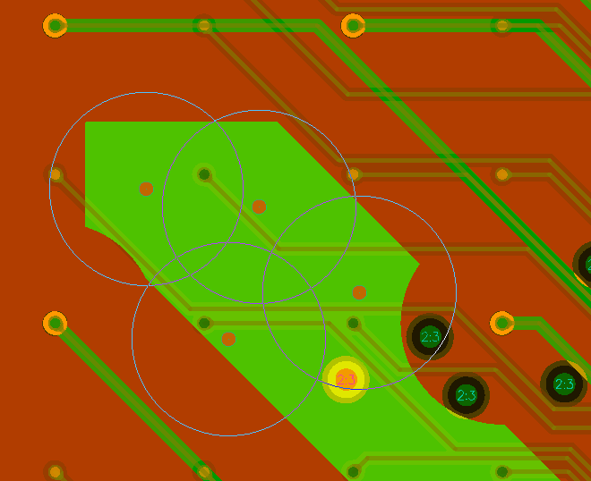
Figure 8. As voids are added, circles show the effective radius.
Green areas needing a void, and adjacent layers are shown
Dummy metal fill
Another metal balancing method utilized on interposer designs with high-bandwidth-memory (HBM) or RDL interconnects is dummy fill. Dummy fill refers to unconnected metal shapes. This can reduce capacitance and help increase manufacturing yield. It can be multi-pass with multiple shapes that can grow to a set maximum length. It can also be density aware and add fill to hit a target value.
Utilizing a density analysis tool that allows visualization of the density windows in the host layout tool is para- mount to find and fix areas and layers that do not meet the vendor rules.
In any of these methodologies you will need to simulate to make sure that the solution meets your performance specification. While foundries and OSATs are focused on manufacturability and yield, it falls to the user to ensure compliance with the performance specification. You must simulate your power delivery before you dismiss an outgassing methodology. At first glance, having signals crossing a plane area with hundreds of voids like we saw in the earlier example might sound like a bad idea: however, it can behave similarly to solid fill and may not present any issues. Without PDN simulation, you’re just guessing at its suitability.
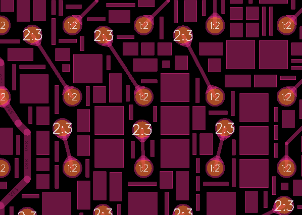
Figure 9. Multi-pass density aware dummy fill
Analysis using the appropriate methodology will ensure that the design meets performance specifications. Recommended types of analysis include DC drop (voltage drop, current density, via currents), PDN impedance analysis, and signal integrity analysis, including return path checks.
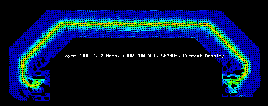
Figure 10. Tightly coupled return currents flowing on the cross hatched plane layer underneath the trace
Conclusion
In summary, dynamic hatched fill, outgassing voids, and dummy metal fill are the most common methods to achieve foundry/OSAT requirements for metal areas and planes. The key is choosing the methodology that best meets vendor rules, meets your PDN specifications, allows rapid ECO turns, and is repeatable. To expedite verification, make sure you turn on dynamic cross-probing between the vendor sign off tool and the layout tool.
Kendall Hiles is a
Also Read:
Connecting SystemC to SystemVerilog
Today’s SoC Design Verification and Validation Require Three Types of Hardware-Assisted Engines
Resilient Supply Chains a Must for Electronic Systems
Share this post via:


Comments
There are no comments yet.
You must register or log in to view/post comments.