 In a complex semiconductor market today, characterized by ever increasing design size and complexity, long design cycle, rapid technological advancement, intense competition, pricing pressure, small window of opportunity, development and cross-functional teams spread across the globe and multiple design partners including several IP vendors for a single SoC, it’s essential for a corporate to identify key strategies for its sustainable competitive advantage. Among so much divergence in the ecosystem, there need to be some key elements of convergence to unify the system and provide direction to achieve goals at the right time of opportunity and in cost effective manner. Unified design data management is one such activity which is immensely important for the success of any semiconductor organization because such an organization handles large design data from various sources which gets revised or modified by multiple teams and is reused frequently.
Dassault Systemes group offers ENOVIA Synchronicity DesignSync Data Manager which brings compelling value to any semiconductor organization from technical, commercial and economical perspectives. It manages design data throughout the product life cycle; from specification, development, test and release, and follow on releases thereafter. Although I knew about DesignSync, didn’t realise that it silently works behind the scene and keeps the companies ahead in time-to-market until I read a paper on its ROI impact analysis done by Gantry Group by interviewing a group of ENOVIA’s 18 top customers. I would not go into the details of that study, however a summary of what customers liked about ENOVIA’s DesignSync is in the following table –

These inputs indicate that DesignSync is a critical enabling technology infrastructure for semiconductor and electronics companies to sustain their competitive advantage. As I realised after going through the paper, some of the key advantages of using DesignSync are –
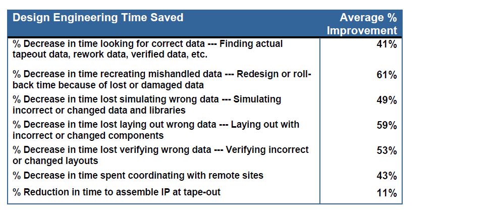
Design Flow Efficiency – By embedding DesignSync into design flows, companies are able to automate the whole process of data management and version control to bring consistency in the design without bothering designers for this mundane but essential work. The design engineering time saved as a result of DesignSync was estimated as –

Design Engineer Productivity – No wonder, design engineer productivity is improved in several ways such as designers’ time spent in producing higher number of gates, increased product throughput, reduced team size, seamless handling of larger number of design configurations and shorter integration cycle. Quantitative figures for these are mentioned in the paper.
Getting back to tape-out configuration – When silicon comes back from the fab, DesignSync enables engineers, spread across multiple sites, to quickly pick up from where they left off in the design, hence saving enormous time-to-market for the company.
Data Set Compares – It’s extremely helpful for an enterprise wide team, distributed across geography to quickly and automatically figure out the design changes between different versions of a design within seconds.
Saving in Disk Space – It provides great relief for designers not to bother keeping multiple local copies of their design work. DesignSync instils confidence among designers for safe handling and retrieving of their design data in a unified manner without any duplication thus consuming only the required disc space. This is a boon for today’s semiconductor business where design data size itself can be in terabytes.
IP Re-use – As DesignSync supports modular design structure, it becomes easy to maintain and re-use IP modules in the designs. Use of IP is a significant strategy for semiconductor organizations.
There are other advantages; notably, ease of collaboration among teams spread across multiple sites, reduced product cost, predictable and optimized project schedules and reduced probability of failures. A reduction in re-spin of mask set (a 65 nm mask set could cost up to $2M) can save millions of dollars.
The paper also records some of very impressive quotes from Dassault’s customers who rightly saw the advantage of using DesignSync; managing consistency in data, handling seamless collaboration in enterprise wide teams, enabling to achieve project deadlines, Hierarchical Configuration Management and so on. Interested audience can take a look at the complete paper at –
ROI Impact Analysis of ENOVIA Synchronicity DesignSync® Data Manager, even try using DesignSync, if not used earlier.
To gain more info – visit Dassault’s booth #1625 at DAC 2013, Austin, TX – June 2 – 6
As a concluding remark, I would like to mention that semiconductor industry is one which continued investment in R&D even at a time of economic slowdown to gain edge in technology innovation. As a result, we are talking about 14nm and 10nm process nodes today. In such a fierce competition and $$ at stake, it’s wise to have a companion like DesignSync which helps eliminating every wastage of time, money and energy to keep the design teams and companies ahead on their goals.
Share this post via:


Musk’s Orbital Compute Vision: TERAFAB and the End of the Terrestrial Data Center