The rapidly increasing complexity of today’s designs, combined with schedule pressure to deliver innovative products to market as quickly as possible, strains engineering resources to the limit, often to the point of breaking. As a result, 17% of all projects get canceled, and another 28% miss their target release date (Source: Lifecycle Insights – September, 2018). Project health is suffering. A more efficient design flow is needed to better utilize available engineering resources, while keeping complex projects moving forward on schedule.
The key to a more efficient design flow is the early detection and elimination of potential design issues. These potential issues can range from simple schematic errors allowed to propagate forward into layout, to complex mechanical issues, to issues impacting product testability and manufacturability. Identifying and fixing these potential issues as early in the process as possible avoids unnecessary schedule delays and costly design re-spins. It also frees up valuable engineering talent to move on to other projects.
The Conventional Design Flow
The traditional project development flow is inefficient and fraught with pitfalls. It relies far too heavily on manual reviews and costly prototypes. Verification of each design phase occurs far too late in the process. Valuable engineering resources are spent debugging errors in the lab that should have been caught during schematic entry. Errors uncovered this late in the game result in costly re-spins, that once again follow the same inefficient, error prone, manual review process.
As a result of this conventional process flow, the typical project goes through 2.9 re-spins, with an average schedule hit of 8.5 days and a cost of $44,000 per re-spin (Source: Lifecycle Insights – September 2018). For high-performance designs, the costs are often much higher. Due to the complexities of modern designs, these delays and added costs are unpredictable and project managers tend to bake them into their schedules and budgets. This conventional approach wastes time, talent, materials and puts projects at risk for cancelation.
The Shift-Left Approach to Integrated Design Verification
In order to eliminate the inefficiencies of the conventional design flow, a “shift-left” approach is desired that integrates verification as early as possible in the design process. This means catching errors and potential issues at the source, before they can propagate forward into subsequent phases of the project. Schematic errors should be caught during schematic entry, not in the lab after building costly prototypes and hundreds of hours of debug time. Automated schematic integrity analysis should be employed to eliminate the reliance on manual, visual schematic reviews.
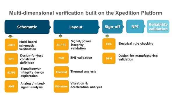
Routing constraints for signal and power integrity, as well as design for test constraints should be specified during schematic capture, not shoe-horned in at the layout phase. Signal and power integrity, EMI compliance, thermal analysis and vibration analysis should all be validated during the layout process.
The goal of the shift-left approach is the same in all cases – to move as much verification as possible as early in the design cycle as permissible, while also automating the analysis to provide the highest possible degree of coverage. The conventional design flow is frustratingly unpredictable. It relies far too much on manual visual design checks that allow far too many errors to propagate forward to the next step in the process. The shift-left verification flow catches errors and identifies potential issues early in the process where they are quickly and economically corrected. It is a more efficient process that provides more predictable results, eliminates design re-spins and yields higher quality products in less time. The ultimate goal should be an all-inclusive, multi-dimensional verification process that reduces reliance on both manual reviews and manual debugging of physical prototypes.

A Multi-Dimensional Verification Solution
A multi-dimensional verification solution is comprised of a broad range of analysis and verification tools used during the schematic and layout phases of the project. These tools are aimed at non-specialist PCB design engineers and layout designers and allow them to work within their familiar authoring environments to identify problems early in the design.
During schematic capture automated schematic integrity analysis is performed to eliminate common schematic errors that often escape the manual review process. Signal integrity and power integrity analysis is performed to determine a set of placement and routing constraints to be passed forward to layout. Testability analysis should also occur during schematic entry, prior to layout. The design is analyzed, test point requirements are identified and passed to layout as constraints.
During layout, as component placement is progressing, EMI validation, thermal analysis, vibration/acceleration and manufacturability analysis should all be performed to quickly identify and correct any potential issues. In the traditional design flow, these issues would not be discovered until physical testing in an EMI, thermal or HALT test chamber. If they are not caught during layout, issues that impact the mechanical integrity of the design are usually the most expensive and time consuming to fix. Such issues often require board re-spins and tooling changes to correct. Simulations during layout greatly increases the likelihood of first-pass success.
The Tools to Implement a Shift-Left Automated Verification Design Flow
The Mentor® Xpedition® platform includes all of the shift-left enhancements described in this article. Xpedition provides a multi-dimensional integrated verification platform for single and multi-board PCB designs that includes automated schematic integrity analysis with built-in automated design checks and an extensive library of intelligent models. Xpedition also includes integrated testability analysis, automated component modeling for vibration analysis, DC voltage drop analysis for rigid-flex and multi-board designs, as well as concurrent DFM analysis during layout.
Xpedition provides powerful verification tools integrated within the authoring environment to enable easier, faster validation which reduces costly design re-spins, improves time-to-market for new products and results in higher quality product with fewer defects. The Xpedition integrated verification platform is a better, more modern approach to today’s complex design challenges.
For more information, read Integrated Verification: A Shift-Left Solution for a More Efficient Design Flow.


Comments
2 Replies to “Eliminate PCB Re Spins using an Integrated Multi Dimensional Verification Platform”
You must register or log in to view/post comments.