 Light is a form of energy. It reveals an object’s color and shape through the refraction (passing through light) or the reflection (bouncing back light) of its beam. While photon is the smallest measure of light, the term photonicscan be defined as the science and technology of generating, controlling, and detecting photons.
A unique characteristic of light is its speed. Speed signifies time and is a common denominator to many technological applications including IC designs. According to Einstein’s theory, the speed of light is the ultimate measure of an object’s speed in the universe. Emerging technologies such as AI-of-Things (AIoT), nano-technology, self-driving vehicles and 5G have driven an increased demand in data center’s compute speed and bandwidth –which in turn, have pressed the urgency of reducing data latency and motivate further exploration of photonics based solutions to improve data speed.
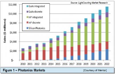 A subset of photonics, integrated photonics, deals with optical signal modulation and detection on an IC. Its market segments which include sensors, networking, self-driving cars and hyperscale data centers are growing as shown in figure 1. Two years ago, the total market size of integrated photonics has exceeded the discrete segments’ and has continued its trend ever since.
The state of interconnect technology
Today’s IC design still has a major reliance on the use of copper for both global and local interconnects. Although recent technology scaling has hit a plateau, both foundries and design teams have been actively seeking alternatives to improve data transport both on-chip and off-chip. As the physical characteristics of the wires dictate their performance, the present mitigation approaches include segregating metal layers for high-speed need (global nets) versus slower intra-cells (local interconnection), and is considered inadequate to satisfy advanced data center application requiring speed migration now tilting towards 400Gb/s.
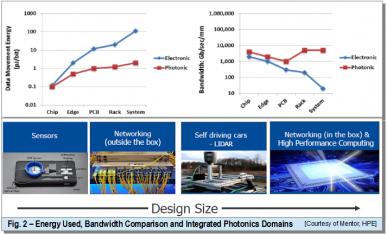
As illustrated in figure 2, photonics based solution provides a better option as it offers a higher bandwidth, better energy efficiency and low latency –all traits suitable for addressing interconnect bottleneck.
Photonics related challenges and solution
Our quest in harvesting light as energy source has been quite successful as reflected in the mainstream adoption of renewable energy through solar cells. How about applying photonics for interconnect? Harnessing its potential for data movement is challenging as it ventures into multiple domains. As opposed to CMOS or FinFET based designs, the layout forms of photonic structures including their interconnects, are mostly non-Manhattan-ic.
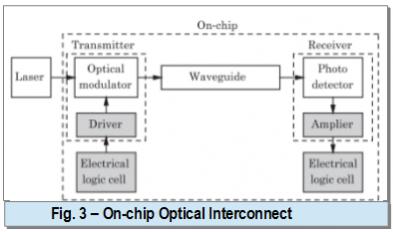 Amidst many photonics application, fiber optic is becoming the key medium for light transport as it needs few repeaters, has ample bandwidth/capacity and is immune to electromagnetic interference. In addition, it is hard to tap without being detected. An example of an on-chip application involves the use of source components (modulator, laser), waveguide and receiver (sensor) as illustrated in figure 3.
“Photonic chips promise amazing performance, but designing circuits today is just too difficult and requires specialized knowledge,” said M. Ashkan Seyedi, Ph.D., senior research scientist, Hewlett Packard Enterprise. His view was also confirmed by others in the system supply chain. “Both silicon development and optics development takes a long time, typically 2-3 years from start of product development,” said Andy Bechtolsheim, chairman and co-founder of Arista Networks.
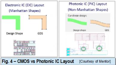
From the EDA standpoint, Tom Daspit, Product Manager at Mentor Graphics, shared a similar view, “Photonic designers are not IC designers. You need more IC design knowledge to do photonics design. More IC layout knowledge is also needed for integrated photonics…unlike the orthogonal CMOS design.“ In addition, physical verification tools need to be revamped as curved structures trigger false DRC errors, complex LVS device recognition and optical property comparison.
To address such photonic design challenges, Mentor, a Siemens business, recently announced the availability of LightSuite™ Photonic Compiler –the industry’s first integrated photonic automated layout system. LightSuite enables designing integrated photonic layouts by capturing the designs in the Python language, from which the tool then automatically generates designs ready for fabrication. The design implementation is guided by Mentor’s Calibre® RealTime Custom verification tool.
“Mentor’s LightSuite Photonic Compiler represents a quantum leap in automating what has up to now been a highly manual, full-custom process that required deep knowledge of photonics as well as electronics… Mentor is enabling more companies to push the envelope in creating integrated photonic designs.” said Joe Sawicki, vice president and general manager of the Design-to-Silicon Division at Mentor, a Siemens business.
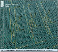
Added Ashkan Seyedi of HPE, “LightSuite Photonic Compiler fixes the biggest roadblocks preventing industry-wide adoption of electro-optical design and simulation of photonic chips. LightSuite Photonic Compiler circumvents those challenges and enables scalability. I’m thrilled to have worked with Mentor to develop this tool to make it possible for anyone to design and build photonic circuits as easily as designing electronic circuits.”
Before and after LightSuite
Prior to LighSuite, photonic designs are very involved and rudimentary. It includes the use of analog, full-custom IC tools to create photonic designs, manually place the components from a process design kit (PDK) and manually interconnect those components with curved waveguides. Furthermore, a full Calibre physical verification needs to be run to check for design rule violations. This can easily translate to DRC fixes and iterations.
As Lightsuite Photonic Compiler (LPC) is designated for handling photonic layout, designers have complete control of their layouts and easily perform automatic placement and route of both the photonic and electrical components. The setup amounts to creating a Python script to drive LPC. An initial placement can also be defined in either Python format or as a pre-placed OA (Open Access) design.
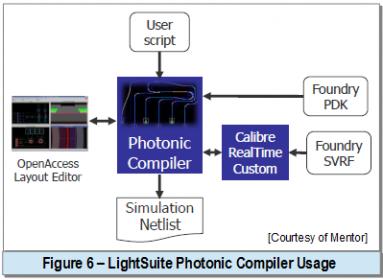
During LPC subsequent interconnect completion step, simultaneous electrical components route and photonics components hook-up with curved wave guides are done. With Mentor’s Calibre RealTime Custom integrated under-the-hood, designers can run LPC in interactive mode –with a Python IDE as the cockpit and the Viewer as output visualization facility. LPC uses Calibre RealTime Custom during the inner placement and routing loop, yielding a design-rule correct layout or “Correct by Calibre”. Furthermore, LPC enables designers to perform quick “what-if” design exploration, which traditionally was prohibitive. A comparative analysis between the manual approach versus LPC based on a 400 component photonic design shows a photonic cost saving (2 weeks versus 9 minutes)!.
Photonics foundry support currently includes AIM photonics, CEA Leti and is to be expanded to cover Smart Photonics, TowerJazz and Advanced Micro Foundry. For more details on Mentor’s LightSuite Photonic Compiler, please check HERE
Share this post via:


Comments
3 Replies to “LightSuite – Physical Design Goes Photonics!”
You must register or log in to view/post comments.