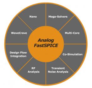
In working with TSMC and GlobalFoundries on AMS design reference flows I have experienced first hand the increasing verification challenges of nanometer analog, RF, and mixed-signal circuits. Tools in this area have to be both silicon accurate and blindingly fast! Berkeley Design Automation is one of the key vendors in this market and this blog comes from discussions with BDA CEO Ravi Subramanian. I first met Ravi at the EDAC CEO Forecast panel I moderated in January, he is probably the only EDA CEO that spends more time in Taiwan than I do!

When analog/RF/mixed-signal IC design meets nanometer CMOS geometries, the world changes. Analog/RF circuit complexity increases as more transistors are used to realize circuit functions; radically new analog circuit techniques that operate at low voltages are born, creating new analysis headaches; digital techniques are mixed into analog processing chains, creating complex requirements for verifying the performance of such digitally-controlled/calibrated/assisted analog/RF circuits; more and more circuits need to operate where devices are in the nonlinear operating region, creating analysis headaches; layout effects determine whether the full-potential of a new circuit design can be achieved; and second and third order physical effects now become first-order effects in the performance of these circuits.
Circuit simulation remains the verification tool of choice, but with little innovation from traditional analog/RF tool suppliers, designers are forced to fit their design to the limitations of tools – breaking down blocks into sizes that lend themselves to easy convergence in transient or periodic analysis, using linear approximations to estimate the performance of nonlinear circuits, ignoring the impact of device noise because of the impracticality of including stochastic effects in circuit analysis, characterizing circuit performance for variation without leveraging distribution theory, and cutting corners in post-layout analysis because of the long cycle times in including layout dependent effects in circuit performance analysis.

In the face of all of this, design flows are being retooled to leverage the best in class technologies that have emerged to solve these new problems with dramatic impact on productivity and silicon success. Retooling does not mean throwing out the old and bringing in the new – rather it is an evolutionary approach to tune the design flow by employing the best technology in each stage of the flow that will remove limitations or enable new analyses.
On September 22[SUP]nd[/SUP] at TechMart in Santa Clara key EDA vendors will showcase advanced nanometer circuit verification technologies and techniques. Hosted by Berkeley Design Automation, and including technologists from selected EDA, industry and academic partners, this forum will showcase advanced nanometer circuit verification technologies and techniques. You’ll hear real circuit case studies, where these solutions have been used to verify challenging nanometer circuits, including data convertors; clock generation and recovery circuits (PLLs, DLLs); high-speed I/O, image sensors and RFCMOS ICs.You’ll hear real circuit case studies, where these solutions have been used to verify challenging nanometer circuits, including data convertors; clock generation and recovery circuits (PLLs, DLLs); high-speed I/O, image sensors and RFCMOS ICs.
I hope to see you there! Register today, space is limited.
Share this post via:


Silicon Insurance: Why eFPGA is Cheaper Than a Respin — and Why It Matters in the Intel 18A Era