

 Verifying circuits on advanced process nodes has always been difficult, and it’s no easier with today’s nanometer CMOS processes. There’s a great paradox in nanometer circuit design and verification. Designers achieve their greatest differentiation when they implement analog, mixed-signal, RF and custom digital circuitry on a single nanometer CMOS die, running at GHz frequencies. Yet it’s these very circuits that create huge design challenges, and introduce a whole new class of verification problems that traditional approaches can’t begin to adequately address.
Fortunately there’s a group of companies bringing to market innovative solutions that focus exactly on these problems, and collaborating to hold the nanometer Circuit Verification Forum (nmCVF), on September 22[SUP]nd[/SUP] at TechMart in Santa Clara. Hosted by Berkeley Design Automation, and including technologists from selected EDA, industry and academic partners, this forum will showcase advanced nanometer circuit verification technologies and techniques. You’ll hear real circuit case studies, where these solutions have been used to verify challenging nanometer circuits, including data convertors; clock generation and recovery circuits (PLLs, DLLs); high-speed I/O, image sensors and RFCMOS ICs.

In addition to technical presentations and case studies, renowned EDA industry veteran and visionary, Jim Hogan, will give the keynote address.
Schedule
9:00- Registration
9:30- Welcome and Keynote
10:00- Morning sessions (including break)
12:30- Lunch
1:30- Afternoon sessions (including break)
4:30- Solution demonstrations and reception
6:30 – Forum wrap-up and close
Topic Areas
Application Examples
– Data converters
– PLLs and timing circuits
– High-Speed I/O
– Image sensors
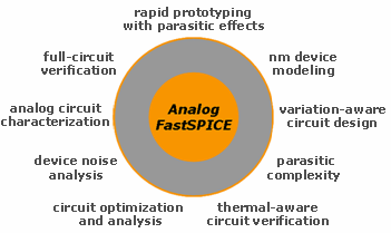
Emerging Verification Technologies
– Nanometer device modeling
– Rapid prototyping including parasitic effects
– Thermal-aware circuit verification
– Variation-aware circuit design
– Circuit optimization and analysis
You should plan to attend if you’re a practicing circuit designer or a hands-on design manager, and you’re looking for high-integrity and comprehensive circuit verification solutions, focused on improving your circuit and getting it faster to market and faster to volume production.
Register HEREfor the nanometer Circuit Verification Forum, or see nm-forum.comfor more details. This event is FREE so you know I will be there!


Silicon Insurance: Why eFPGA is Cheaper Than a Respin — and Why It Matters in the Intel 18A Era