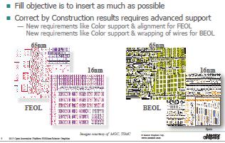
To describe the latest methodology for the addition of Design for Manufacturability fill shapes to design layout data, it’s appropriate to borrow a song title from Bob Dylan – The Times They Are A Changin’. The new technical requirements are best summarized as: “The goal is now to add as much fill as possible, which (ideally) looks like the actual design.”
At the recent TSMC Open Innovation Platform symposium, Zhe Lui from HiSilicon and Bill Graupp from Mentor Graphics presented results of their collaboration with TSMC to optimize the fill database for a HiSilicon N16 design. Specifically, Mentor and TSMC enhanced the algorithms in Mentor’s Calibre YieldEnhancer with Smart Fill tool (and the DFM Data Kit runsets), while Mentor and HiSilicon implemented a hierarchical methodology for managing the additional data volume and subsequent design verification runtimes.
Background
The addition of fill data for DFM originated with the Chemical-Mechanical Polishing (CMP) process for improved BEOL metallization planarity. To reduce the extent of metal line “dishing” during polishing, a rule for minimum local metal density measured across a small stepping window was established, and metal fill algorithms were implemented to meet this requirement.
The shapes were typically of a size/spacing to have minimal impact on electrical performance. The shapes were added “at the end, in the top cell” of the design, to meet tapeout criteria. That has all changed…
Current fill data requirements
Fill data must now meet a much more stringent set of lithography requirements – e.g., stepping window density (as before), density gradient limits, multi-patterning decomposition “color assigned” fill data, color-specific density on a layer.
No longer solely a methodology to address BEOL metal thickness uniformity after CMP, fill data is now directly related to:
- lithographic uniformity of FEOL layers (especially for FinFET processes)
- induced mechanical stress on devices (affecting their electrical characteristics)
- etch rate uniformity (from the “loading” of material to be removed)
- electrical behavior (due to the proximity of fill data to design data)
As a result, the volume of fill data required has exploded – “often greater than 1B shapes/layer, or 3-4X the size of the design database”, according to Mentor and HiSilicon. The full-chip (flat fill) DRC verification resources alone quickly became intractable.
Hierarchical fill

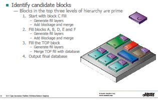
Mentor and HiSilicon developed a hierarchical “fill as you go” methodology, starting with lower-level cells. This necessitated enhancements to the Calibre YieldEnhancer Smart Fill algorithms. Optimizations were required at the perimeter of cells – “no empty space”. Interconnects were “wrapped” with fill data to match multi-patterning color assignments.

HiSilicon described the engineering approach needed to implement hierarchical fill:
- (lower-level) cell selection
- addition of blockage layers for subsequent fill steps
- the flow for layout database management

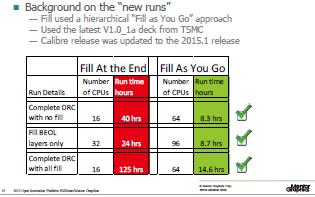
This new methodology deployed at HiSilicon enabled them to maintain suitable turn-around time in final full-chip verification.
(Although HiSilicon and Mentor didn’t explicitly mention this feature in their presentation, Calibre Smart Fill also includes algorithmic support for ECO fill, a key feature required to keep the verification and analysis iteration time for a last-minute design change in check.)
As Moore’s Law proceeds, the complexity of DFM requirements will certainly continue to grow. This OIP presentation highlights that a foundry + EDA vendor + design company collaboration is extremely beneficial to drive tool and methodology enhancements, to address these complexity challenges. The times they are (definitely) a changin’…
-chipguy
Share this post via:


Comments
0 Replies to “Meeting DFM Challenges with Hierarchical Fill Data Insertion”
You must register or log in to view/post comments.