The ability to extend photolithography utilizing 193i light sources to current process nodes is truly the key technical achievement that has enabled Moore’s Law to continue. The interplay between the exposure equipment, the materials – especially, resists and related coatings – and the fundamental principles of optics is complex, and also fascinating.
In the early deep submicron process nodes, “optical proximity corrections” (OPC) were made to the original mask data, to enhance the fidelity of the photolithography process – e.g., “serifs” added at shape corners to reduce line end pullback. At the 22nm process node and beyond, a detailed analysis of the entire optical system is required. The printing of the target design data requires optimization of the source illumination pattern together with the corresponding mask data – aka, “Source Mask Optimization” (SMO).
Neal Lafferty, Director of SMO Development at Mentor Graphics, was gracious enough to educate me on the recent advancements in this field. As part of the breadth of Mentor’s Calibre product family, pxSMO, pxOPC, and OPCVerify are the tools used for source and mask data generation, and final verification of “printability”. These tools are key to both initial process development and production fabrication.

During development, process integration engineers run SMO/OPC experiments on wafer test runs, to guide development of the layout design rules. The rules reflect the tradeoff between the goals of high circuit density and manufacturing yield, due to variations in both process and photolithography steps. The Design Rule Manual component of the production Process Design Kit (PDK) release is the culmination of these early experiments. Subsequent customer tapeout layer data are also analyzed using these tools, to create the production masks and corresponding illumination source patterns.
Neal indicated that the current 193i exposure equipment provides highly-programmable “pixelated” light sources, utilizing an independently-addressable multi-mirror array. The ability to propagate (plane wave) illumination with different angles provides many degrees of freedom for the pxSMO transform algorithms. The light source pattern is optimized to compensate for the diffractive elements in the overall system – e.g., the mask chrome pattern, the (thick glass) mask itself, the photoresist and coating materials, and any nonlinearities in the optical path. Light sources have definitely come a long way, from in-axis uniform intensity, to off-axis quadrupole illumination, to the current state-of-the art with programmable pixelated patterns.
To determine the quality of the SMO solution, the Mentor tools utilize “gauges” and “clips” in the layout data. A measurement gauge is a feature of the layer data where the critical dimension (CD) is a key process control parameter – e.g., a device gate length, a metal line width, a contact or a cut mask opening. The gauges are defined by the process integration engineer.
From the layout data, specific clips are selected, typically ~1-2um on a side. In practice, a design mask layer might utilize ~10-20 clips for SMO optimization. A clip might contain up to a few hundred gauges. Clips may be defined manually (painstakingly!), or auto-selected by a new feature incorporated into the Calibre toolset. Additionally, the tools provide settings that toggle whether specific gauges are to be omitted from consideration during the SMO data generation phase, to save computation time.
After the light source pattern and mask data are generated, a subsequent OPCVerify analysis will evaluate all gauges for their printability. (OPCVerify also cleans up the generated mask data, removing vertices that are immaterial to the printed image.)
The simulated exposure for each gauge after SMO is analyzed, and a quantitative calculation of the quality of the image for all gauges is made. The process integration engineer provides the set of metrics for each gauge, and the relative weight associated with each measure – e.g., the light intensity (dose), the slope of the intensity at a line edge (contrast), the depth of focus. The engineer can run multiple SMO experiments with different weighting factors on these metrics, and compare the results to select the preferred source pattern and mask data.
Neal highlighted that this layer clip + gauge analysis methodology is applicable to any layout style, whether a highly periodic array or a very asymmetric (logic-like) layout – although more gauges may be appropriate for the latter case.


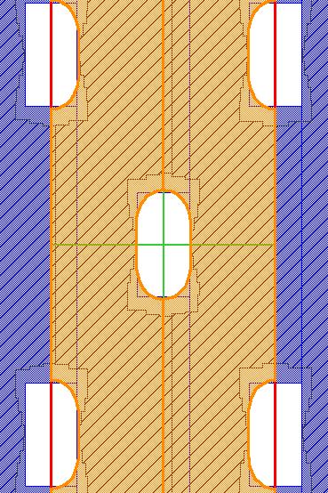
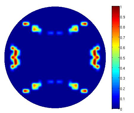
The figure briefly illustrates an example of SMO results, for a layout with an array of mask data openings. The rectangle in the very center of the clip is the typical drawn layout shape. The green lines in the center of the rectangle are the gauges (in both directions), across which the simulated image result will be analyzed. The detailed, multi-edge shape around the drawn shape is the final mask data, with the corresponding illumination source pattern. The orange oval is the nominal, simulated image for the opening.
Parenthetically, designers at current process nodes are now required to exercise a lithography process checking (LPC) step prior to tapeout, using a tool such as Mentor’s LFD and an encrypted runset from the foundry’s design kit. During process integration development, the wafer run experiments on the film stacks, resists, masks, and illumination sources will require iterations with pxSMO/pxOPC and OPCVerify optimizations. The production OPCVerify step serves as the basis for the LPC runset released in the design kit, for the required pre-tapeout lithographic analysis.
Neal briefly mentioned that EUV lithography presents new challenges to SMO, due to the unique transition to reflective optics, and the unique pattern of the EUV source. He described EUV illumination as “more like points of light… discrete samples across the field… yet, the EUV mask shadowing effects are understood, and of course, the laws of optics haven’t changed.” 🙂
Indeed, there is a long history and a wealth of experience at Mentor with RET, and SMO technology in particular. Mentor will continue to provide both the fundamental computational lithography technology and the ease-of-use features to allow foundries, IDM’s, and equipment/materials providers to manage the complexity and challenges of lithography at new process nodes.
A technical article that provides additional detail on pxSMO/pxOPC/OPCVerify is available from Mentor’s web site, at this link.
-chipguy
Share this post via:


Comments
There are no comments yet.
You must register or log in to view/post comments.