 I was talking recently to Dina Medhat, a senior technical marketing engineer at Mentor, about, of all things, IO rings. It has not occurred to me that verifying that your IO rings comply with foundry rules presents new challenges.
IO ring checking isn’t new, nor is it unique to advanced IC process nodes. However, the same forces of complexity and physics are in play in all aspects of IC design, requiring careful consideration when planning IO pad rings. Medhat says there is a distinct need for a robust, automated flow to do IO ring checking. She told me about some of these challenge and what she’s been doing to create an automated LEF/DEF-based IO ring checking flow that is flexible and can target different foundries.
Consider that designs typically include IP from multiple vendors, and each vendor has its own set of rules. One important goal of pad cell placement is good electrostatic discharge (ESD) protection when co-locating dissimilar types of cells, such as digital logic, analog cells, processor cores, IO power pads, IO ground pads, termination cells, and so on. Evaluating the design against the many different IP rules, and more especially the rule interactions, depends on automated checking. The remaining question for design teams is how to set up such a flow.
First, says Medhat, let’s look at what the foundries provide—a design rule manual (DRM) with guidelines for pad cell placement that guarantee the required ESD protection when using a given library. Designs must follow these rules when digital, analog, core input, and output (IO) power and ground pads are placed in an IO ring. Common rules that you see in DRMs include:
- Cell types that can be used in an IO ring
- Minimum number of a specified power cell per IO ring section and given power domain
- Maximum spacing between two power cells for a given power pair in a power domain
- Maximum distance from the IO ring section termination to every power cell
- Maximum distance from IO to closest power cells
- Maximum continuous IO ring section of filler without any interruption (breaker or dummy ESD cells)
- Cells that must be present at least once per corresponding power domain section
- Constraints for multi-rows implementation
The obvious question is “How can I make sure that my design is safe and that I applied all these rules correctly?” A more subtle question is “Are the rule constraints for these cells the same for all IPs and all foundries, or are they cell- and foundry-specific? If they are different, how do I handle this complexity in an automated flow?”
 Of course, constraints are different from one foundry to another, as well as from one technology node to another, and one IP supplier to another. Complying with all of these rules is extremely important, but it’s not easy, and it’s not something you want to do manually. Designers need an automated solution to ensure compliance and improve ESD protection in their designs, but it must also be flexible enough to handle all the details and variations without overwhelming the design team with rule coding, says Medhat.
As with most IC design technologies these days, the ‘ecosystem’ code word applies. The EDA vendors must work with their customers to establish an automated framework to verify compliance with the foundry’s IO placement rules. Medhat has recently spent a fair amount time demonstrating the practicality of this approach using Calibre PERC on real customer designs.
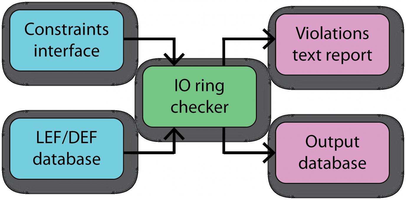
“The input are LEF/DEF files, and all the common rules are already coded in our IO Ring Checker framework,” says Medhat. “Users define their unique constraints using the constraints interface (input form), which is part of the framework, then point to their LEF/DEF database. Executing the IO Ring Checker framework generates two outputs: a violations text report and a violations database, both of which can be loaded into a results viewer like Calibre RVE to debug violations graphically.”
The IO Ring Checker is pretty new, which is why Medhat is presenting results at the DAC Work-In-Progress session on Wednesday evening, June 10, from 6:00-7:00 pm. Look for “LEF/DEF IO Ring Check Automation” (86.65).
Are any of you are incorporating automated techniques for IO ring checking? If so, what techniques are you using, and what are your challenges, results, best practices?
Share this post via:


Comments
There are no comments yet.
You must register or log in to view/post comments.