Having spent a significant amount of my career in EDA and IP I can tell you first hand how important picking the right prototyping partner is. I have known S2C since my interview with CEO Toshio Nakama in 2017. It has been a pleasure working with them and I look forward to seeing an S2C update at DVCon the first week of March here in Silicon Valley. Specifically I am looking forward to seeing the new Prodigy Logic System.

The Prodigy S8-100 Logic System-VP1902 is a high-performance FPGA-based prototyping platform designed to accelerate advanced System-on-Chip (SoC) and ASIC development in demanding applications such as AI, high-performance computing (HPC), networking, and RISC-V processor design. Built and marketed by S2C Inc., a leader in FPGA prototyping solutions, the S8-100 series harnesses the latest AMD Versal™ Premium VP1902 adaptive SoC as its core building block. This integration enables developers to prototype large-scale digital logic designs with unprecedented gate capacity and I/O flexibility compared to previous generations of prototyping systems.
At its core, the Prodigy S8-100 platform is about bridging the gap between RTL design and full hardware validation before production silicon is available. FPGA prototyping has become essential because software development, validation, and system-level debugging often cannot wait for the final ASIC to be manufactured. The S8-100’s modular architecture enables hardware teams to test, refine, and validate entire SoCs—right down to peripheral interfaces—on reconfigurable hardware. Unlike simple simulation environments, this FPGA-based approach allows real execution of logic under real timing conditions, enabling much earlier detection of integration bugs and performance bottlenecks.
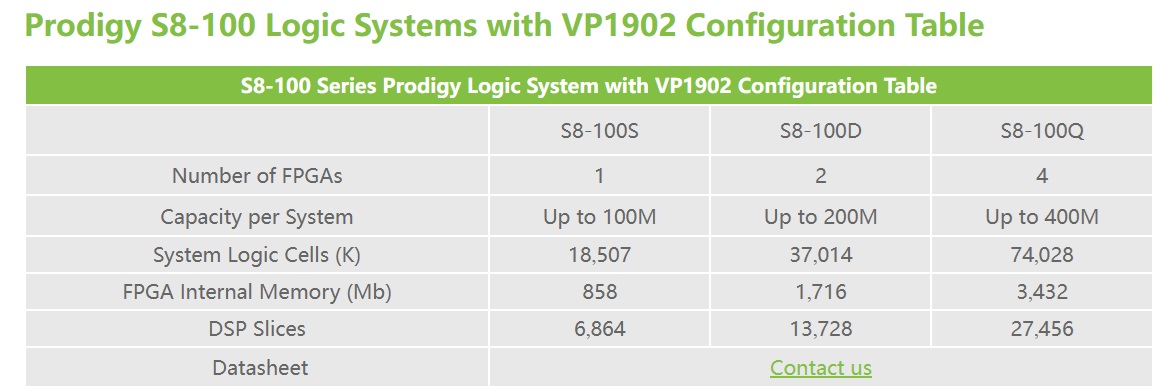
A defining feature of the Prodigy S8-100 is its massive logic capacity, with each VP1902 FPGA supporting up to 100 million ASIC equivalent gates.
Systems can be configured in three variants:

In multi-FPGA configurations, the total effective capacity scales up to 400 million gates, providing headroom for extremely complex designs that incorporate multiple cores, accelerators, memory hierarchies, and communication fabrics.
Resource-wise, the S8-100 offers rich internal capabilities including tens of thousands of logic cells, megabits of on-chip RAM, and thousands of DSP slices per FPGA. It also boasts advanced I/O support with high-speed transceivers and contemporary interface standards such as PCIe Gen5, enabling real-world connectivity with host systems and other devices. The result is a prototyping system capable of both high throughput and real-world system integration testing.
Beyond raw hardware, the Prodigy S8-100 ecosystem includes a suite of productivity tools to streamline prototyping workflows. S2C’s software, including PlayerPro-CT for partitioning and ProtoBridge for co-simulation, helps automate complex multi-FPGA design partitioning and bitstream generation. An extensive catalog of “Prototype Ready IP” daughter cards further expands the platform’s usability, offering pre-validated interface modules (for memory, Ethernet, GPIO, and more) that plug into the system without consuming valuable FPGA logic. These tools together reduce setup time, simplify board bring-up, and allow teams to concentrate on verification and software development instead of hardware plumbing.
The Prodigy S8-100 is also gaining traction in emerging markets such as RISC-V SoC development, where developers need to validate not just CPU cores but entire subsystems that include custom extensions and accelerators. In a recent collaboration with Andes Technology, the S8-100 platform has been used to prototype advanced RISC-V designs with custom instructions and high-bandwidth interfaces, demonstrating its value in next-generation CPU and SoC workflows.
Bottom line: The Prodigy S8-100 Logic System-VP1902 represents a state-of-the-art prototyping solution that addresses the challenges of modern digital design: huge logic capacity, flexible I/O, scalable configurations, and robust toolchains. For semiconductor developers working on cutting-edge chips—from AI accelerators to custom processors—platforms like the S8-100 make it possible to validate complex designs thoroughly, accelerate software readiness, and reduce the risk associated with first-silicon prototypes. As design complexity continues to grow, FPGA-based prototyping systems like the Prodigy S8-100 will remain essential tools in the semiconductor development cycle.
Also Read:
S2C, MachineWare, and Andes Introduce RISC-V Co-Emulation Solution to Accelerate Chip Development
FPGA Prototyping in Practice: Addressing Peripheral Connectivity Challenges
S2C Advances RISC-V Ecosystem, Accelerating Innovation at 2025 Summit China
Share this post via:


Comments
There are no comments yet.
You must register or log in to view/post comments.