


Designing semiconductor chips has traditionally been costly and controlled by a few major Electronic Design Automation (EDA) vendors—Cadence, Synopsys, and Siemens EDA who dominate with proprietary tools protected by NDAs and restrictive licenses. Fabrication also requires expensive, often export-controlled equipment. This oligopoly raises barriers for small companies, researchers, and students.
A growing movement is shifting towards free and open-source EDA tools and open Process Design Kits (PDKs) that lower costs, broaden access, and foster innovation. Open EDA can be applied partially for simulation or across the entire design flow from concept to fab-ready layout. While most advanced nodes still require proprietary PDKs, open PDKs for older nodes (e.g., SkyWater 130 nm, IHP 130 nm, GlobalFoundries 180 nm, ICSprout 55 nm) enable ASIC production without NDAs.
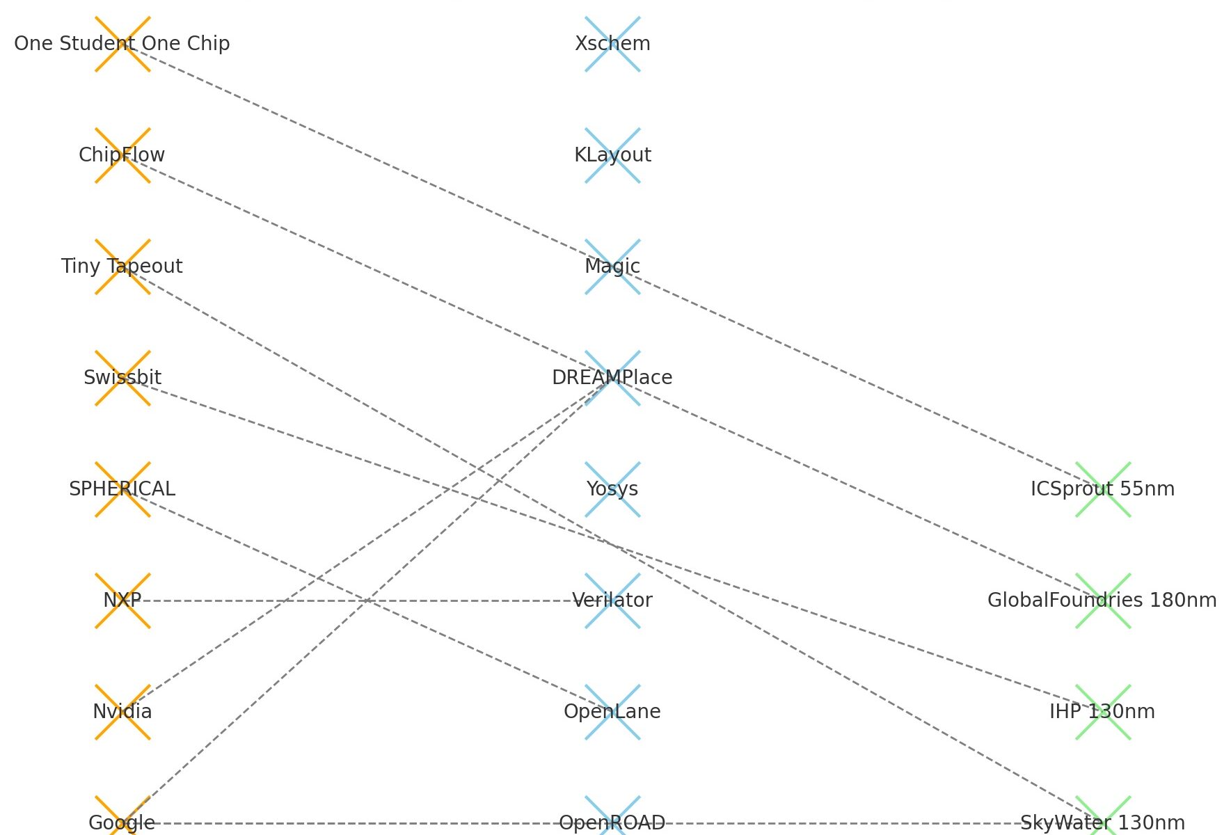
Illustrated uses span education, research, and industry:
-
Commercial adoption: Google, Nvidia, and NXP use tools like Verilator (fast open-source simulation) and DREAMPlace (timing optimization) in production workflows. SPHERICAL applies open tools to design radiation-hardened chips for satellites; Swissbit integrates open, provably correct cryptographic modules.
-
Educational outreach: Initiatives like Tiny Tapeout and One Student One Chip let thousands of students produce working ASICs for as little as $300, using open PDKs.
-
Emerging products: Automotive ECUs, high-speed serial links, and gaming consoles are being prototyped with open flows.
Advantages and opportunities include:
-
Cost reduction: Proprietary EDA licenses can cost $10k+ per workstation per month. Open tools slash entry costs, enabling low-volume and niche ASIC designs to be profitable.
-
Innovation: Open frameworks allow modification, integration of AI-based design aids, and rapid iteration, often impossible in closed systems.
-
Security: Open designs and tools can be audited, mathematically verified, and built to standards like Caliptra, reducing risks of hidden hardware Trojans or backdoors. Transparent, community-verified cryptographic modules enhance trust.
-
Education and skills: Students can install and explore open EDA freely, enlarging the future talent pool in semiconductor design.
Challenges remain significant:
-
Performance gap: Open tools may lag behind commercial software in supporting advanced nodes, analog/mixed-signal, or mm-wave designs.
-
PDK access: Leading-edge fabs (e.g., TSMC N3) will likely never open their PDKs, limiting open EDA’s reach to legacy and mid-range processes.
-
Commercial risk: For high-value ASICs, companies may prefer proven proprietary flows to minimize costly re-spins.
-
Coordination vs. fragmentation: Efforts like OpenROAD (US), iEDA (China), and Coriolis (France) may duplicate work or compete rather than pool resources.
The paper outlines strategic options:
-
For investors: Experiment internally with open tools, join cost-sharing consortia (CHIPS Alliance, Linux Foundation), and explore hybrid flows mixing open and proprietary components.
-
For governments: Fund open PDK development, secure fabrication options, and support international cooperation—even across geopolitical lines—to build technological sovereignty.
Security-driven innovation is a standout theme. Openness enables formal verification of hardware components, provably secure random number generators, and side-channel-resistant designs. These can be deployed in “trusted” or even open fabs, forming verified value chains from chip design to system integration.
The future of open EDA could follow several paths:
-
Remain primarily educational, producing small ASICs for learning.
-
Emerge as a viable commercial competitor to the “Big Three,” especially for mid-range nodes.
-
Blend into hybrid flows, where open tools augment proprietary ones.
-
Drive creation of transparent, standardized fabs with openly shared process data.
Bottom line: While barriers exist, the trend appear, per UCSD’s Andrew Kahng, “unstoppable and irreversible.” As more companies and governments seek cost-effective innovation, security assurance, and independence from proprietary lock-in, free and open EDA is poised to expand its role in global semiconductor development.
The original paper from HEP Alliance is here.
Also Read:
WEBINAR: Functional ECO Solution for Mixed-Signal ASIC Design
Taming Concurrency: A New Era of Debugging Multithreaded Code
Perforce Webinar: Can You Trust GenAI for Your Next Chip Design?
Share this post via:


Musk’s Orbital Compute Vision: TERAFAB and the End of the Terrestrial Data Center