By Hossam Sarhan
Communication has become the backbone of our modern world, driving the rapid growth of the integrated circuit (IC) industry, particularly in communication and automotive applications. These applications have increased the demand for high-performance analog and radio frequency (RF) designs.
However, designing analog and RF circuits can be quite challenging due to their sensitivity to various factors. Changes in layout design, operating conditions, and manufacturing processes can all have a significant impact on circuit performance. One of the major hurdles faced by analog designers is the issue of noise coupling between interconnects.
The proximity and interactions between different circuit elements can lead to signal noise, which can degrade the overall circuit performance. This is a critical concern, as analog and RF circuits are more susceptible to proximity effects, such as crosstalk and coupling noise, compared to their digital counterparts.
Mitigating noise coupling with net shielding
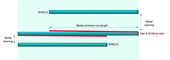
One of the widely used techniques to protect critical nets in analog and RF circuit designs is net shielding. This approach involves surrounding the sensitive signal nets with power or ground nets, which create a shielding effect that helps mitigate the impact of electromagnetic interference and crosstalk on the critical signal traces.
The power and ground nets, with their stable and low-noise characteristics, act as a barrier to isolate the critical signals from noise sources. This shielding helps maintain the integrity of the sensitive signals, preventing unwanted noise and disturbances. Figure 1 illustrates net shielding.

Additionally, the geometries belonging to the same net, when placed in close proximity to each other, can also act as a form of self-shielding. The proximity of the same-net traces creates a shielding effect, further protecting the critical signals from external interference.
By employing net shielding techniques, circuit designers can effectively safeguard the performance and reliability of analog and RF circuits, ensuring that the critical signals are isolated from noise sources and maintain their intended behavior.
Verifying net shielding effectiveness
Verifying the effectiveness of net shielding is not a straightforward task, as it requires tracing the critical net segments and checking the surrounding nets to confirm how much of the victim net is shielded. This process can be time-consuming and error-prone if done manually.
To address this challenge, designers can adopt an advanced reliability verification platform that provides comprehensive net shielding verification. A solution like Calibre PERC from Siemens EDA offers a packaged checks framework for net shielding verification that automates the verification process, streamlining the design validation workflow. This framework permits simple selection and configuration of pre-coded checks, maximizing ease-of-use and minimizing runtime setup. Calibre PERC packaged checks are provided as well dedicated checks to enhance the reliability of analog circuits.
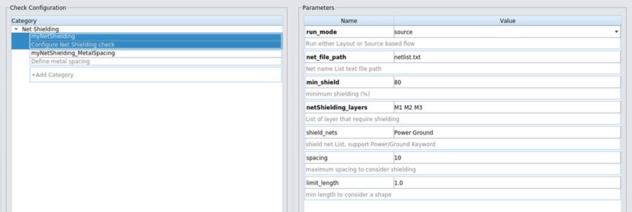
The input for the packaged checks flow is a user configuration file with specified checks and their parameters. This input constraint file is processed by a package manager, which accesses the checks database and creates a rule file containing all of the selected checks, with the proper configuration parameters to run on the designated design. Figure 2 shows the net shielding setup using Calibre PERC packaged checks GUI.

Advance net shielding checks allows designers to specify the critical nets in their design and the minimum shielding percentage threshold required. The verification tool then automatically traces each critical net, analyzes the surrounding shielding nets and calculates the shielding percentage for each net.
The verification results can be viewed and cross-probed in the layout to help with debug.
By leveraging automated net shielding verification, designers can quickly and reliably validate the effectiveness of their net shielding implementation, ensuring that the critical signals are adequately protected from noise sources. This streamlined approach helps designers identify and address any net shielding issues, enhancing the overall reliability and performance of their analog and RF circuits.
The key benefits of using an advanced net shielding verification tool include:
- Automated verification: The platform’s dedicated net shielding check eliminates the manual and error-prone process of tracing net segments and calculating shielding coverage, saving designers significant time and effort.
- Streamlined integration: The platform’s packaged checks framework allows designers to easily integrate net shielding verification into their overall design validation flow, enabling them to combine multiple reliability checks into a single validation run.
- Improved reliability: By quickly and reliably validating the effectiveness of net shielding implementation, the advanced platform helps designers identify and address any issues, ensuring the overall reliability and performance of their sensitive analog and RF circuits.
Conclusion
Protecting critical signals from noise coupling is a crucial aspect of successful analog and RF circuit design. Net shielding is a widely used technique that involves surrounding sensitive signal nets with power or ground nets to create a shielding effect, mitigating the impact of electromagnetic interference and crosstalk.
However, verifying the effectiveness of net shielding can be a challenging task. Fortunately, solutions exist. Designers can easily adopt an advanced reliability verification platform to provide automated and streamlined net shielding verification. With the right tools, designers can quickly identify and address any issues, ultimately enhancing the reliability and performance of their analog and RF designs. Packaged shielding net checks help designers deliver delivering high-quality products that meet the demanding requirements of today’s communication and automotive applications.
About the author:
Hossam Sarhan is a senior product engineer in the Design to Silicon division of Siemens Digital Industries Software, supporting the Calibre PERC reliability platform and Calibre PEX tools. His current work focuses on circuit reliability verification and inductance parasitics extraction. Prior to joining Siemens, he worked in modeling and design optimization for on-chip power management circuits. Hossam received his B.Sc. from Alexandria University, Egypt, his M.Sc. degree from Nile University, Egypt, and his Ph.D. from CEA-LETI, Grenoble, France.
Also Read:
Revolutionizing Simulation Turnaround: How Siemens’ SmartCompile Transforms SoC Verification
Siemens EDA Unveils Groundbreaking Tools to Simplify 3D IC Design and Analysis
Jitter: The Overlooked PDN Quality Metric
Share this post via:


Comments
There are no comments yet.
You must register or log in to view/post comments.