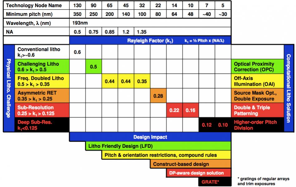
The first part of Lars Liebmann’s ICCAD keynote about lithography was on the changes in lithography that have to us to where we are today. In some ways it was an explanation of why we have the odd design rules, double patterning etc that we have in 20nm and 16nm processes. The second part of his talk was a look forward to how we might be able to go further.
Once again, here is the Rosetta Stone of Lithography, a summary of how lithography affects EDA at each process node all in one table.
The first approach that we can use down to 7nm is pitch multiplication. For some layers at earlier process nodes we need to use self-aligned double patterning (SADP) or sidewall image transfer (SIT). But we can use this technique twice to get quadruple patterning. This is known as self-aligned quadruple patterning (SAQP) or as SIT[SUP]2[/SUP]. The basic idea is that a mandrel is put down, as with SADP, and the sidewalls are deposited and the mandrel removed. But now we do it again, and use those original sidewalls as new mandrels, and deposite sidewalls on the sidewalls and remove the original sidewalls/mandrel. This gives us a grating at 4 times the pitch we can achieve with the basic optical (which is 80nm). Theoretically this would be 20nm but in practice is is more like 30nm.
The second approach is directed self assembly (DSA). I’ve written about this before. The basic idea is to take two polymers that won’t mix like oil and water. If they are just deposited on the wafer then you get a random pattern a bit like a fingerprint. However, if some guide layout is already in place, then the polymers line up in a neat tight grid that can then be divided up with a cut mask. It is resolution in a bottle. A few years ago this was a novelty that looked unlikely to be of any practical relevance, but with increasing investment and experiments it is starting to look increasingly practical.
The third approach, that I have also written extensively about, is extreme-ultra-violet (EUV). This is using 14nm light (versus 193nm that we have been using for the last decade). There are a lot of challenges with EUV but here are the ones I think are the most significant:
- intensity of the light source. EUV is generated by zapping droplets of molten tin with a huge laser. But currently the intensity of the light is not enough to get a wafer throughput that is high enough to be economically competitive
- EUV is absorbed by everything including lenses and air. So the entire system needs to be in a vacuum and we need to go to reflective optics, not refractive. In fact normal mirrors also absorb EUV so we need mirrors that are made up of layers of silicon and molybdenum. These reflect about 30% of the incident EUV so only about 2% of the EUV generated at the source makes it to the photoresist on the wafer
- EUV masks have defects. It is impossible to see the defects until the multiple layers of the mirror are constructed and then it is too late. But the bottom line is that it is not possible to guarantee that masks are defect free
- There is no pellicle on an EUV (reflective) mask since it would absorb the EUV. So unlike in refractive optics, any contamination on the mask will be in the focal plane and will print
The big challenge going forward is that increasingly it looks like we will only be able to lay down regular gratings and then use a cut mask to divide them up. The big question is whether that is good enough for us to be able to design the kind of structures that we need on the silicon. The big problem layer is first metal since it is very difficult to design standard cells with first level metal being unidirectional. There is local interconnect (which is contactless and just connects to everything it crossed) but there are lots of challenges, especially in power delivery.
More articles by Paul McLellan…


Silicon Insurance: Why eFPGA is Cheaper Than a Respin — and Why It Matters in the Intel 18A Era