The current Coronavirus crisis is inflicting a lot of pain on people, companies, and governments. I hope I am not getting in trouble with my reasoning, but if you look closely, there are also some “positives” to the Covid-19 crisis.
– It is stress-testing our infrastructure and telling us where we need to improve – as country, states, communities, companies, and individuals – to benefit long-term.
– Empty shelves and/or purchase quantity limits at grocery stores show us the importance of a solid supply chain.
– Extremely high demand for laptops, iPads, video cameras, and other essentials for working remotely, tell us that High-Tech is a great industry to work for and that we have a lot of opportunities for growth – if we get the pricing right.
Allow me to pick up on “getting the pricing right” and outline some ideas how to streamline the High-Tech supply chain, to further lower the cost of electronic products, make it easier to set up home offices and grow our revenues and profits.
From 1980 until ’96 I worked in the manufacturing part of the semiconductor supply chain, at two big IC vendors. Since 1997 I am in the Electronic Design Automation (EDA) portion, focused on encouraging the use of EDA tools to make semiconductor manufacturing more efficient and more cost-effective, by broadening the collaboration between EDA and manufacturing experts.
EDA and wafer foundry experts have made remarkable progress in the last forty years. For example: in 1980 I sold my first ASIC at two cents per gate; today two cents buy you at least one Million gates. Excellent collaboration between material suppliers, equipment vendors, wafer foundries as well as EDA, IP and IC design experts made such progress possible.
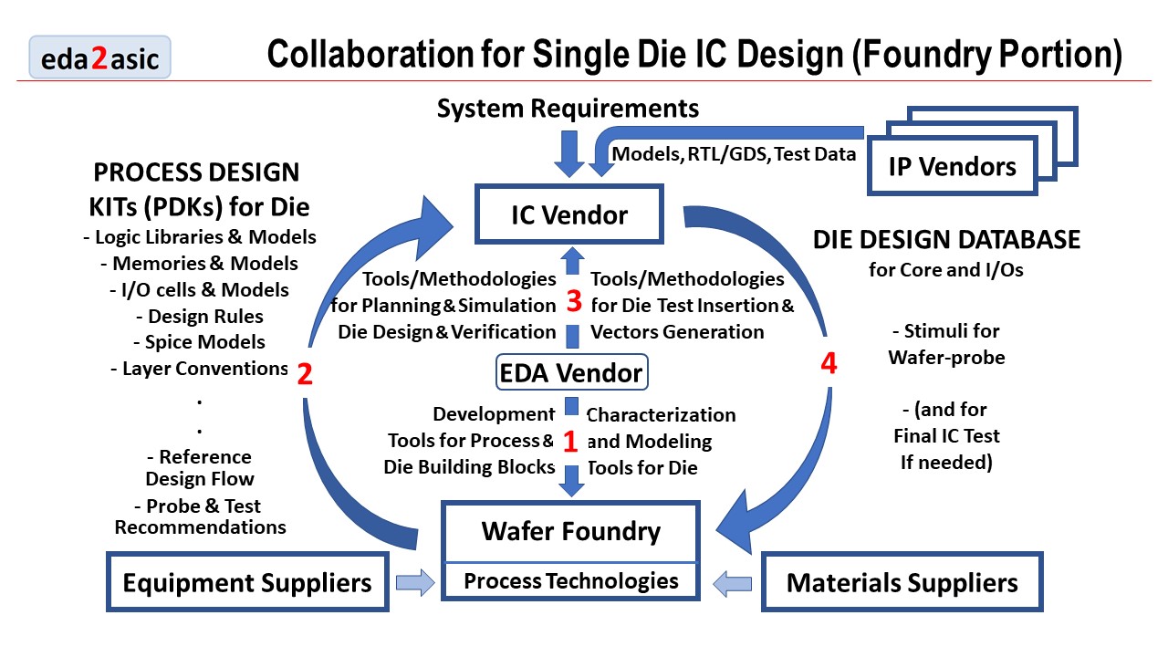
Figure 1 shows a significantly simplified Collaboration Flow between the essential parties. They have enabled in the last four decades enormous IC complexity increases, broadened the range of functionalities and, at the same time, reduced cost per function by six orders of magnitudes.

Figure 1 Collaboration with Foundry
During the 2008 financial crisis, rumors about the end of Moore’s Law and the need for More than Moore started. I took this as an opportunity to change my focus from the traditional single-die SoC technology to multi-die ICs (2.5/3D-ICs). In these new technologies the package adds a lot of value to the complete solution. Until that time, I was used to being part of the broad and in-depth cooperation between EDA vendors and wafer foundries, developing Process Design Kits (PDKs) and Reference Design Flows. That’s the reason why I was surprised that IC assembly/test houses (a.k.a. OSATs), at that time, were not as proactive as wafer foundries. They had no design kits, nor reference flows, and the excellent engineers at the OSATs had to spend a lot of manual efforts, to meet their customers’ IC packaging and cost requirements.
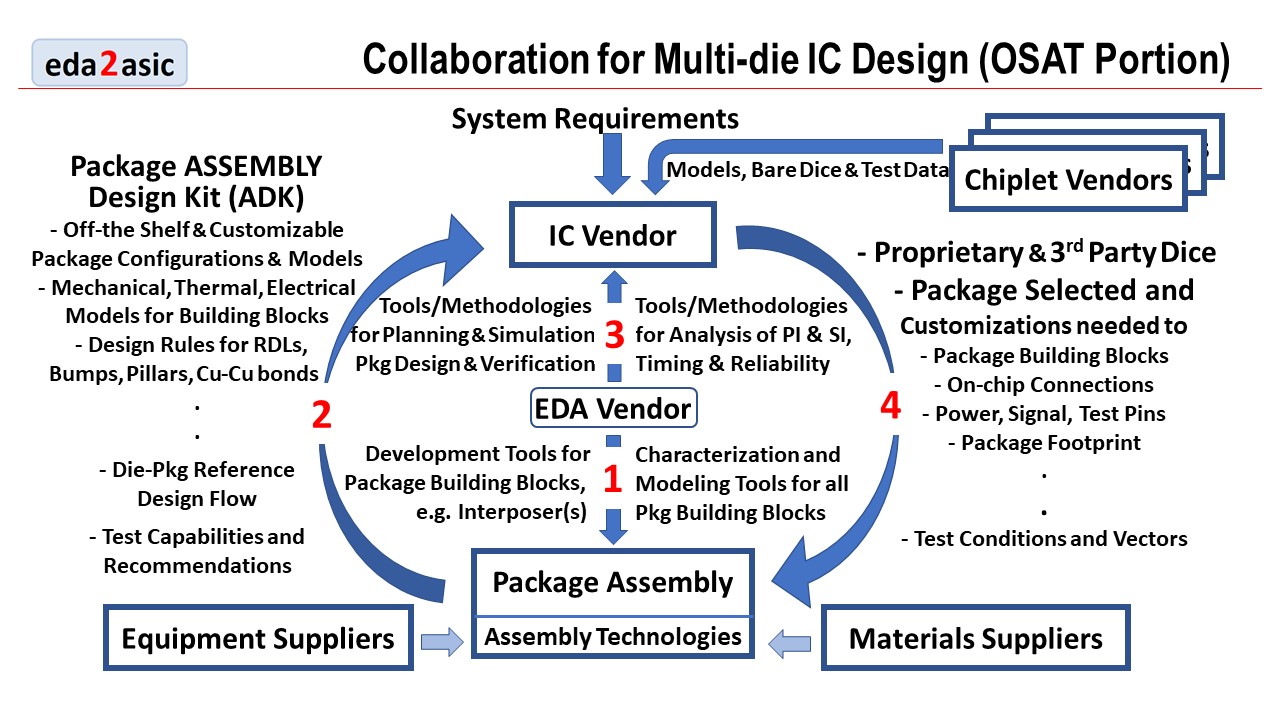
Thanks to industry organizations, like the Global Semiconductor Alliance (GSA), SEMATEC, the Silicon Integration Initiative (Si2), the Electronic System Design Alliance (ESDA), MEPTEC and SEMI, who gave me “a soap-box” to better highlight the industry’s pressure for more automation between IC designers and OSATs, several OSATs have developed since, in cooperation with their EDA partners, Assembly Design Kits (ADKs) and Design Reference Flows for packages. Figure 2 shows a significantly simplified Collaboration Flow between the essential parties, to reduce package development time and engineering cost. Please, DO NOT plan on six magnitudes in package unit cost reduction. To achieve this target, IC packages would need to be shrunk so much, that nobody could see or use them anymore.

Figure 2 Collaboration with OSAT
Bottom Line: Assembly Design Kits and Design Reference Flows encourage the use of off-the-shelf or “pre-customized” packages. Yes, they do limit IC designers’ flexibility somewhat, but the significant savings in development time and engineering cost, as well as lower manufacturing cost will reward IC Vendors and OSATs royally for streamlining/automating their collaboration. Best of all, ADKs and Reference Flows make IC package design and manufacturing very scalable!!!
Share this post via:


Musk’s Orbital Compute Vision: TERAFAB and the End of the Terrestrial Data Center