ASIC prototyping in FPGAs is starting to trend on SemiWiki. As FPGA technology becomes more advanced customers tell me that the traditional debug tools are inadequate. Faced with the very restrictive debugging capabilities and very long synthesis/place/route times the debugging cycle in these prototype platforms are quite long and painful.
SemiWiki has been writing about a tool from Tektronix called Certus. This tool has been adopted by several of the top semiconductor companies because it addresses long debug cycles through advanced capabilities that are orders of magnitude better than existing tools in several dimensions.
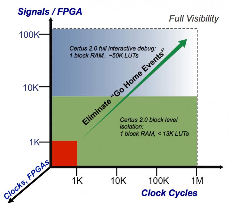
The Certus ASIC Prototype Debug tool has significant competitive advantages versus other offerings. The differentiation is rooted in Certus’s unique and patent pending observation network. The figure below quantifies how this solution is multiple orders of magnitude better in three dimensions compared to existing ASIC Prototype debug solutions.

In order to develop a truly compelling solution, the Certus team had to develop several industry firsts:
- the only one that enables full visibility which eliminates most FPGA synthesis-place-route cycles.
- the only solution that provides time correlation of data across multiple clock domains and devices.
- The only solution with real-time compression of captured data enabling capture of full startup sequences and system wide events.
The ability to fully instrument a multi-FPGA prototype with a dozen large FPGAs enables users to debug their hardware rapidly under real-world stimulus. Because of the visibility advantage, development teams can then provide the prototype platform for their software and firmware groups with the instrumentation intact to enable rapid debug of hardware/software bugs and to optimize system performance by analysis of performance bottlenecks.
Certus fundamentally changes the FPGA prototyping flow and dramatically increases debug productivity. By leveraging Certus full RTL-level visibility and making internal visibility a feature of the FPGA prototyping platform, an engineer can diagnose multiple defects in a day where it would take them a week or more with existing tools.
A major challenge today is that traditional FPGA debug tools are unable to support the requirements of the ASIC prototyping market, particularly as designs have become larger and span multiple FPGA devices. Add the increased complexity of hardware/software interactions and the high-speed operation of most prototypes, and FPGA debug has become a major bottleneck in the ASIC prototyping process. Now, by using Certus 2.0 to pre-instrument up to one hundred thousand signals per FPGA device, designers gain comprehensive RTL-level signal visibility without time consuming synthesis and place and route cycles, allowing complex problems to be pinpointed and resolved quickly.
Those who are interested in learning more can send an email request to eig-info@tektronix.com for white papers or demos at DAC.
lang: en_US
Share this post via:


Musk’s Orbital Compute Vision: TERAFAB and the End of the Terrestrial Data Center