I recently spoke to Arvind Narayanan, Product Marketing Manager for Mentor’s place and route division about emerging technology. This of course led to FinFETS, FDSOI, performance, power, and cost-benefit. The battle between FDSOI and FinFETs, said Narayanan, is going to be something to watch.
Both FDSOI and FinFET technologies provide better performance better power than bulk CMOS process. But, Narayanan asked, how do they compare with each other? Will FDSOI at 20nm bridge the 16nm finFET gap? Does finFET offer better cost benefits than FDSOI? The jury is still out on these questions, but he has some thoughts from a P&R perspective.
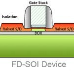
 FDSOI technology relies on a thin layer of silicon that lays over a Buried Oxide (BOx). Transistors are built into the thin silicon layer, which is fully depleted of charges. Because the body is fully depleted the random dopant fluctuation that plagues bulk CMOS is reduced, thus improving performance even at lower VDD.
Some companies experimenting with FDSOI claim it has roughly 30% better performance, and lower power use, than bulk CMOS at 28nm.
28nm FDSOI is positioned as an alternate to bulk CMOS at 20nm. Narayanan said that if 28nm FDSOI delivers even half the power savings of bulk 20nm, it would be worth going that way to avoid dealing with the expense of double patterning (which is needed at 20nm). He pointed to another cost and scheduling benefit of 28nm FDSOI over 20nm FinFET from a P&R perspective; the FDSOI technology can use the conventional design flows and is completely transparent to the design tools.
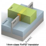
 FinFET also promises the sun and the moon in terms of power, performance, and area. FinFET devices have their channels turned on their edge with the gate wrapping around them. The term “fin” was coined by professors at Berkeley to define the thin silicon conducting channel. This unique configuration of a gate wrapped around the channel on all three sides delivers much better channel control and better resistance to dopant fluctuations. The innovative 3D structure and tighter channel control does result in improved area, better performance, and lower power than bulk CMOS. Narayanan said that the P&R flows should be minimally affected by the adoption of FinFET devices, but that FinFET is more difficult to design and manufacture. FinFET technology is in production at 22nm and is quickly ramping up for the next generations.
Narayanan can’t predict whether one of these two technologies will actually become dominant, or if they both find a niche and co-exist successfully. As always, he said, production volumes with determine the eventual winner.
You can find related articles on foundry-based IC design and manufacturing at www.mentor.com/solutions/foundry.
Share this post via:


Comments
0 Replies to “For power and performance, Fins or BOXes?”
You must register or log in to view/post comments.