 In the early 1980s the ideas and infrastructure for what would eventually be called ASIC started to come together. Semiconductor technology had reached the point that a useful number of transistors could be put onto a chip. But unlike earlier, when a chip only held a few transistors and thus could be used to create basic generic building blocks useful for everyone, each customer wanted something different on their chip. This was something the traditional semiconductor companies were not equipped to provide. Their model was to imagine what the market needed, create it, manufacture it and then sell it on the open market to multiple customers.
The other problem was that semiconductor companies knew lots about semiconductors, obviously, but didn’t have system knowledge. The system companies, on the other hand, knew just what they wanted to build but didn’t have enough semiconductor knowledge to create their own chips and didn’t really have a means to manufacture those chips even if they did. What was required was a new way of doing chip design. The early part of the design, which was system knowledge heavy, would be done by the system companies. And the later part of the design, which was semiconductor knowledge heavy, would be done by the company that was going to manufacture it.
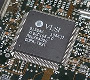
Two companies in particular, VLSI Technology and LSI Logic, pioneered this. They were startup companies with their own fabs (try getting that funded today) with a business model that they would, largely, build other people’s chips. In the early days, since there weren’t really any chips out there to be built, they had to find other revenue streams. VLSI Technology, for example, made almost all of its money building read-only-memories (ROMs) that went into the cartridges for the first generation of video game consoles.
Daisy, Mentor and Valid, who had electronic design systems mostly targeted at printed circuit boards, realized that they could use those systems for the front end of ASIC design too.
ASIC design typically worked like this. A system company, typically someone building an add-on board for the PC market since that was the big driver of electronics in that era, would come up with some idea for a chip. They would negotiate with several ASIC companies to decide which to select, although it was always a slightly odd negotiation since only a vague idea of the size of the design was available at that point. They would then partner with one ASIC company such as LSI Logic who would supply them with a library of basic building blocks called cells.
The system company would use a software tool called a schematic editor to create the design, picking the cells they wanted from the library and deciding how they should be connected up. The output from this process is called a netlist, essentially a list of cells and connections.
Just like writing software or writing a book, the first draft of the design would be full of errors. But with semiconductor technology it isn’t possible to build the part and see what the errors are. Even back then it cost tens of thousands of dollars and a couple of months to manufacture the first chip, known as the prototype. Also, unlike with writing a book, it’s not possible to simply proofread it and inspect the schematic, too many errors would still slip through.
Instead, a program called a simulator was used. A flight simulator tells a pilot what would happen if he or she moves the controls a certain way, and, unlike in the real world doesn’t cost a fortune if the plane crashes. In the same way, a simulation of the design checked how it behaved given certain inputs without requiring the expense of building the chip. Errors that were detected could be fixed and the simulation run again.
 When finally the design was determined to be correct, the netlist was sent from the system company to the ASIC company for the next step. Using a program known as place & route tool the netlist would be converted to a full chip design. In addition to creating the actual layout for manufacture, this process also created detailed timing, just how long every signal would take to change. This detailed timing would be sent back to the system company so that they could do a final check in the simulator to make sure that everything worked with the real timing versus the estimated timing that was used earlier.
At that point the system company took a deep breath and gave the go ahead to spend the money to make the prototypes. This was (and is) called tapeout.
The ASIC company then had the masks manufactured that were be needed to run the design through their fab. In fact there were two main ASIC technologies, called gate-array and cell-based. In a gate-array design, only the interconnect masks were required since the transistors themselves were pre-fabricated on a gate-array base. In cell-based design, all the masks were required since every design was completely different. The attraction of the gate-array approach was that, in return for giving up some flexibility, the manufacturing was faster and cheaper. Faster, because only the interconnect layers needed to be manufactured after tapeout. Cheaper, because the gate-array bases themselves were mass produced in higher volume than any individual design.
A couple of months later the prototypes would have been manufactured and samples shipped back to the system company. These parts typically would then have been incorporated into complete systems and those systems tested. For example, if the chip went into an add-in board for a PC then a few boards would have been manufactured, put into a PC and checked for correct operation.
At the end of that process, the system company took another deep breath and placed an order with the ASIC company for volume manufacturing, ordering thousands or possibly even millions, of chips. They would receive these a few months later, build them into their own products, and ship those products to market. A Brief History of ASIC Part II is HERE.
A Brief History of Semiconductors
A Brief History of ASICs
A Brief History of Programmable Devices
A Brief History of the Fabless Semiconductor Industry
A Brief History of TSMC
A Brief History of EDA
A Brief History of Semiconductor IP
A Brief History of SoCs


Chemical Origins of Environmental Modifications to MOR Lithographic Chemistry