You are currently viewing SemiWiki as a guest which gives you limited access to the site. To view blog comments and experience other SemiWiki features you must be a registered member. Registration is fast, simple, and absolutely free so please,
join our community today!
WP_Term Object
(
    [term_id] => 14433
    [name] => X-Subscriber
    [slug] => x-subscriber
    [term_group] => 0
    [term_taxonomy_id] => 14433
    [taxonomy] => category
    [description] =>
    [parent] => 0
    [count] => 0
    [filter] => raw
    [cat_ID] => 14433
    [category_count] => 0
    [category_description] =>
    [cat_name] => X-Subscriber
    [category_nicename] => x-subscriber
    [category_parent] => 0
    [is_post] =>
)
Much awaited, automatic tool for DRM (Design Rule Manual) and DRC (Design Rule Check) deck creation is here now! I am particularly excited to know about this because I had been hearing for its need (in different context) from the designers with whom I was working to improve their design productivity through the use of our EDA tools… Read More
The tremendous growth in IC and SoC design complexity has now enabled engineers to place bilions of transistors on a single chip. To make that growth possible design teams resort to using libraries and semi IP provided by other groups in their company, or outside IP vendors. To lower risk, you must know that the IP being used in your… Read More
For 19 years GSA (presumably going back to the days when it was Fabless Semiconductor Association, FSA) has recognized public and private semiconductor companies. The awards are celebrated at a dinner. This year’s dinner is on Thursday December 12th at the Santa Clara Convention Center. The keynote speaker at the dinner… Read More
With nearly twenty five years in business, Tanner EDA Application Engineers have seen a wide range of support requests. One consistent topic area is around design data management and design reuse. In one recent instance, our customer, an IDM who produces imaging sensors for infrared vision systems, called on Tanners AE team for… Read More
For a couple of years the GSA has had working group looking at funding of semiconductor investment. There is a general feeling, which I share, that it is hard to get a fabless semiconductor company off the ground (nobody would dream of trying to create one with a fab these days) due to the size of the investment and the relatively long… Read More
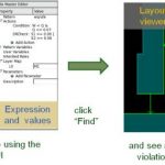
This is an example of what I do during the day. I work with emerging companies on disruptive technologies and help launch them into the fabless semiconductor ecosystem. This product, iDRM, is the result of three years of joint development work amongst three semiconductor foundries and some of their top customers:… Read More
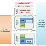
Storage interfaces for mobile are evolving rapidly, in particular with the Universal Flash Storage (UFS) standard. So how do you test a design? If you want to test a design that accesses, say, an SD card then you can wander into Fry’s and buy an SD card for a few dollars. But to design an interface to UFS is a bit harder since the … Read More
Analog and Mixed-Signal (AMS) designers are facing more challenges than ever, so where can they go to get some relief? One place is a half-day seminar scheduled for May 16th in Bridgewater, New Jersey. SemiWiki has teamed up with Tanner EDA, Abbot Labs and SoftMEMS to present topics of:
- True collaborative design enabled through
…
Read More
Very often we talk about increasing design complexities and verification challenges of SoCs. With ever growing design sizes and multiple IPs on a single SoC, it’s a fact that SoC design has become heterogeneous, being developed by multiple teams, either in-house or outsourced. Considering economic advantage amid pressure … Read More
Tanner EDA Applications Engineers see a broad range of technical challenges that our users are trying to overcome. Here’s one worth sharing – it deals with transient noise analysis (TNA) for a comparator design. The customer is a producer of advanced flow measurement devices for application in medicine and research. The designer… Read More