You are currently viewing SemiWiki as a guest which gives you limited access to the site. To view blog comments and experience other SemiWiki features you must be a registered member. Registration is fast, simple, and absolutely free so please,
join our community today!
WP_Term Object
(
    [term_id] => 50
    [name] => Events
    [slug] => events
    [term_group] => 0
    [term_taxonomy_id] => 50
    [taxonomy] => category
    [description] =>
    [parent] => 0
    [count] => 1516
    [filter] => raw
    [cat_ID] => 50
    [category_count] => 1516
    [category_description] =>
    [cat_name] => Events
    [category_nicename] => events
    [category_parent] => 0
    [is_post] =>
)
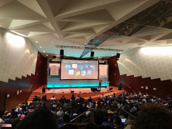
At the Imec technology forum in Belgium, Dan Mocuta and Juliana Radu presented “Evolution and Disruption: A Perspective on Logic Scaling and Beyond”, I also had a chance to sit down with Dan and discuss the presentation.
Device scaling
Scaling of devices will only get you so far, you need to look at new devices and new… Read More
The second Bay Area RISC-V Meetup event was held at the DoubleTree Hilton in Burlingame on June 19 with about 150 attendees. This event was hosted by SiFive and started with a networking session. The topics and speakers for the evening were:
- Commercial Software Tools – Larry Lapides, Imperas
- Securing RISC-V Processors –
…
Read More
The first clue was cloud vendors (Amazon, Google, IBM, etc…) at 55DAC for the first time ever with lots of cloud content including a Design on Cloud Pavilion. The second clue was the pre-briefing from Cadence last week. There has also been a lot of cloud chatter in the semiconductor ecosystem so yes, I saw this coming and EDA will get… Read More
It’s hard to believe that this is the 55th DAC and even harder to believe that this will be my 35th. So much has changed in 35 years, with DAC back in San Francisco I expect a VERY big crowd and even bigger announcements, absolutely.
Not only is this an epic time for semiconductors, I would say that EDA is exciting again and the Mentor… Read More
I’ve been visiting DAC for decades now, at first as an EDA vendor and since 2004 as a freelance EDA consultant. There’s always a buzz about what’s new, semiconductor industry trends, who is getting acquired and the latest commercial EDA and IP offerings. There’s so much vying for my attention at DAC each… Read More
The Design Automation Conference (DAC), now in its 55[SUP]th[/SUP] year, always offers a lively mix of activities. For EDA vendors and their customers, the focus is on the exhibit floor and in booth suites where the latest technology is on display. For R&D engineers and academics, the technical sessions dig deeply into an … Read More
The TSMC OIP DAC Theater schedule is finalized and ready to go. It kicks off Monday at 10:15 am in booth #1629 and ends with a raffle at 5:45 pm each day (Mon-Tue-Wed) TSMC gives out some very nice prizes so check in with the TSMC booth staff when you arrive. There are 66 coveted presentation spots representing the top ecosystem partners… Read More
Design IP is going well, with 12% YoY growth in 2017, even if the market is about $3.5B. But Design IP is serving a $400B semiconductor market. Can you imagine the future of the semi market if the chip makers couldn’t have access to Design IP? The same is true for EDA: it’s a niche market (CAE revenues was about $3B and IC Physical Design… Read More
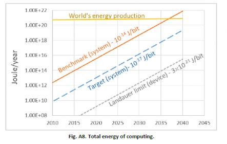
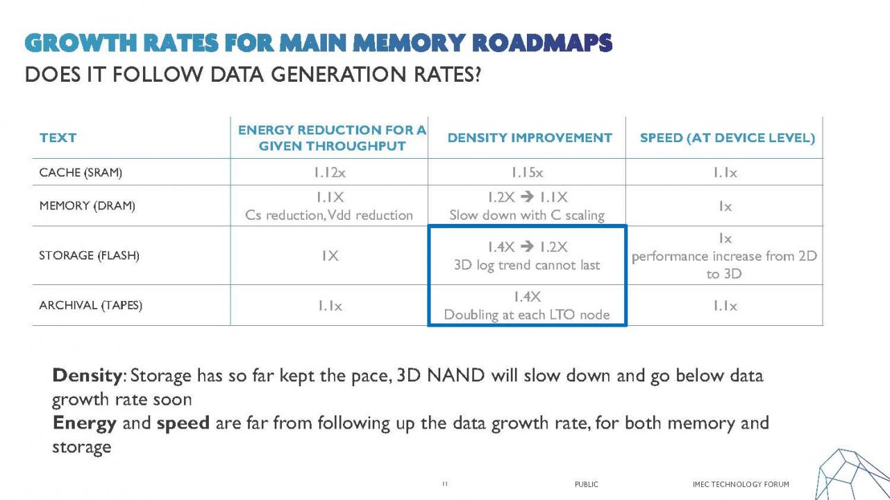
At the Imec technology forum in Belgium Gouri Sankar Kar and Arnaud Furnemont presented memory and storage perspectives and I also got to interview Arnaud. Arnaud leads overall memory development at Imec and personally leads NAND and DNA research.
Memory research is focused on power, energy, speed and cost with energy and throughput… Read More
The 8[SUP]th[/SUP] RISC-V Workshop was held in Barcelona May 7-10 with 325 attendees from 150+ companies and was the biggest RISC-V event outside of Silicon Valley, demonstrating the momentum of the RISC-V Foundation and the growth of the ecosystem in Europe.… Read More


Captain America: Can Elon Musk Save America’s Chip Manufacturing Industry?