You are currently viewing SemiWiki as a guest which gives you limited access to the site. To view blog comments and experience other SemiWiki features you must be a registered member. Registration is fast, simple, and absolutely free so please,
join our community today!
WP_Term Object
(
    [term_id] => 157
    [name] => EDA
    [slug] => eda
    [term_group] => 0
    [term_taxonomy_id] => 157
    [taxonomy] => category
    [description] => Electronic Design Automation
    [parent] => 0
    [count] => 4439
    [filter] => raw
    [cat_ID] => 157
    [category_count] => 4439
    [category_description] => Electronic Design Automation
    [cat_name] => EDA
    [category_nicename] => eda
    [category_parent] => 0
    [is_post] =>
)
Let’s face it, designs are getting harder, much harder. Gone are the days when the electrical and mechanical design of a system occurred separately. Maybe ten years ago this practice was acceptable. Once the electrical design was completed (either the chip or the board) the parameters associated with the design were then given… Read More
Explicit and implicit sneak paths to leak or compromise information continue to represent a threat to security. This paper looks a refinement of existing gate level information flow tracking (IFT) techniques extended to RTL, encouraging early-stage security optimization. Paul Cunningham (Senior VP/GM, Verification at … Read More
The Universal Verification Methodology (UVM) is a popular way to help verify SystemVerilog designs, and it includes a configuration system that unfortunately has some speed and usage issues. Rich Edelman from Siemens EDA wrote a detailed 20-page paper on the topic of how to avoid these issues, and I’ve gone through it to… Read More
Preventing the propagation of systematic defects in today’s semiconductor design-to-fabrication process requires many validation, analysis and optimization steps. Tools involved in this process can include design rule checking (DRC), optical proximity correction (OPC) verification, mask writing and wafer printing… Read More
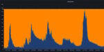
In my previous article, we touched on ways to pull in the schedule. This time I’d like to analyze how peak usage affects project timeline and cost. The above graph is based on real pattern taken from one development week in Annapurna Labs 5nm Graviton.
The Graph shows the number of variable servers per hour per day. There’s a baseline… Read More
The concept of giving back is something many of us have contemplated. Giving back to the community or to support a particular cause. How to respond to those inquiries from our alma mater is another example. These conversations typically focus on giving money to provide needed support. As engineers, we are surrounded by a massive… Read More
At the recent RISC-V Summit, the very last session was a panel about chiplets called Chiplets in the RISC-V Ecosystem. It was moderated by Calista Redmond, the CEO of RISC-V International. The panelists were:
- Laurent Moll, COO of Arteris
- Aniket Saha, VP of Product Management of Tenstorrent
- Dale Greenley, VP of Engineering of Ventana
…
Read More
I knew that HDMI was a popular standard used to connect consumer products like a monitor to a laptop, but most professional video and broadcast systems use the SDI (Serial Digital Interface) connector standard. Pleora Technologies, founded in 2000, currently serves the machine vision and manufacturing markets, including those… Read More
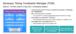
In the world of semiconductor design, constraints are essentially specifications and requirements that guide the implementation of a specific hardware or software component within a larger system. They dictate timing, area, power, performance, and of course functionality of a design, playing a crucial role in ensuring that… Read More
Nowadays, low power design requirements are key for large SoCs (system on chips) for different applications: AI, Mobile, HPC, etc. Power intent management early in the design flow is becoming crucial to help facing PPA (Power Performance Area) design challenges.
WEBINAR REGISTRATION
With the increasing complexity of such … Read More


Chemical Origins of Environmental Modifications to MOR Lithographic Chemistry