You are currently viewing SemiWiki as a guest which gives you limited access to the site. To view blog comments and experience other SemiWiki features you must be a registered member. Registration is fast, simple, and absolutely free so please,
join our community today!
WP_Term Object
(
    [term_id] => 157
    [name] => EDA
    [slug] => eda
    [term_group] => 0
    [term_taxonomy_id] => 157
    [taxonomy] => category
    [description] => Electronic Design Automation
    [parent] => 0
    [count] => 4439
    [filter] => raw
    [cat_ID] => 157
    [category_count] => 4439
    [category_description] => Electronic Design Automation
    [cat_name] => EDA
    [category_nicename] => eda
    [category_parent] => 0
    [is_post] =>
)
Before going to Munich to attend to CDN-Live, I took a look at the agenda to figure out which presentations to attend, and I must say it was not so easy to choose: CDN Live agendais dense, with multiple tracks running in parallel (Custom Design, Digital Implementations, Design IP, Functional Verifications and Verification IP, PCB… Read More
Yesterday’s SEMICO IP Ecosystem Conference was well worth the time. Everybody was there: ARM, Synopsys, Cadence, Mentor Graphics, GlobalFoundries, TSMC, MIPS, Tensilica, AMD, Atrenta, Sonics, and Tabula, everybody except Intel of course. What do Intel and I have in common? We don’t play well with others…
First up was… Read More
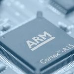
CPAK sounds like something politicians create to collect money, but in fact it is a Carbon Performance Analysis Kit. It consists of models, reference platform, initialization software (for bare metal CPAKs) or OS binary (for Linux and Android based CPAKs). They are (or will soon be) available for ARM Cortex A9, ARM Cortex A15 and… Read More
Yesterday I met with Michael Buehler-Garcia, Director of Marketing at Mentor Graphics for Calibre in Wilsonville, Oregon to get an update on what’s coming up at DAC, the premier conference and trade show for our industry.
… Read More
Cadence Update 2012!by Daniel Nenni on 05-14-2012 at 9:00 pmCategories: Cadence, EDA
What’s new at Cadence? Quite a bit actually. I have always been a Cadence fan, I mean really, they gave birth to modern EDA. Unfortunately, Cadence really lost me during the Avant! legal action, the Mike Fister years, and EDA360. Recently, however, Cadence has made some big changes that will definitely get them back on my good side.… Read More
I am not going to attempt to give you any restaurant advice beyond what I’ve already done by listing the good places near the conference center. San Francisco reputedly has over 3000 restaurants so I don’t know anything about more than a tiny fraction. However, with that many restaurants, most places are pretty good. If not, they … Read More
If you look real close at the #49 DAC floor plan you will see the tiny Intel booth dwarfed by those of TSMC, GlobalFoundries, Samsung, and ARM. The number one semiconductor company in the world does not have the budget for the cornerstone conference of the semiconductor ecosystem? Oh my…… Intel has a big foundry hat and no cattle… Read More
In June I’ll be visiting several first time companies at DAC in order to learn more about what they have to offer in terms of EDA software, then blog about what I discover.
Here’s my list:… Read More
Next month at DAC I plan to visit the ClioSoft booth to get an update on what’s new with hardware configuration management (HCM). Last year I met with Srinath Anantharaman to get an introduction to their company and how their tools are used by both front-end engineers and back-end IC layout designers.
Srinath Anantharaman,… Read More
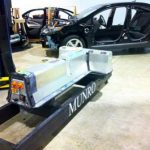
One DAC panel session that I am looking forward to attending is the Chevy Volt Teardown. This takes place at 1.30-2.30pm on Tuesday June 5th at the DAC pavilion (aka booth 310). Al Speier will be talking about a teardown that they did at Munro Associates where he is a senior associate. Unfortunately they won’t actually be tearing… Read More


Silicon Insurance: Why eFPGA is Cheaper Than a Respin — and Why It Matters in the Intel 18A Era