You are currently viewing SemiWiki as a guest which gives you limited access to the site. To view blog comments and experience other SemiWiki features you must be a registered member. Registration is fast, simple, and absolutely free so please,
join our community today!
WP_Term Object
(
    [term_id] => 157
    [name] => EDA
    [slug] => eda
    [term_group] => 0
    [term_taxonomy_id] => 157
    [taxonomy] => category
    [description] => Electronic Design Automation
    [parent] => 0
    [count] => 4365
    [filter] => raw
    [cat_ID] => 157
    [category_count] => 4365
    [category_description] => Electronic Design Automation
    [cat_name] => EDA
    [category_nicename] => eda
    [category_parent] => 0
    [is_post] =>
)
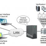
Big SoC designs typically break existing EDA tools and old methodologies, which then give rise to new EDA tools and methodologies out of necessity. Such is the case with the daunting task of verification planning and management where terabytes of data have simply swamped older EDA tools, making them unpleasant and ineffective… Read More
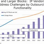
As your SoC design can contain hundreds of IP blocks, how do you verify that all of the IP blocks will still work together correctly once assembled? Well, you could run lots of functional verification at the full-chip level and hope for the best in terms of code coverage and expected behavior. You could buy an expensive emulator to … Read More
By now, you’ve probably seen the news on Synopsys acquiring Coverity, and a few thoughts from our own Paul McLellan and Daniel Payne in commentary, who I respect deeply – and I’m guessing there are many like them out there in the EDA community scratching their heads a little or a lot at this. I’m not from corporate, but I am here… Read More
Mounir Hahad Rejoins Silvacoby admin on 02-20-2014 at 4:16 pmCategories: EDA
Mounir Hahad just joined Silvaco as VP engineering. And when I say joined I really mean rejoined. I had a call with him to find out how that happened.
Mounir studied in France for a PhD in computer science on numerical computing. In 1995 the then-director of TCAD at Silvaco called him up having read some of his published papers. Silvaco… Read More
I’ve run SPICE circuit simulators since the 1970’s and they use transistor models where the device parameters are provided by the foundry. These transistor and interconnect parameters come from an engineer at the foundry who has characterized silicon with actual measurements or by running a TCAD (Technology CAD)… Read More
Synopsys announced this afternoon that they are acquiring Coverity for $375M subject to all the usual reviews.
There are a couple of other big EDA connections. Aki Fujimora, who was CTO of Cadence, is on the board. And Adreas Kuehlmann is the VP of R&D. He used to run Cadence Berkeley Laboratories before moving to the other end… Read More
One SPIE session not to missby Beth Martin on 02-19-2014 at 4:19 pmCategories: EDA, Siemens EDA
The time is nigh for another meeting of the practitioners of the lithographic arts, dark and otherwise, at the SPIE Advanced Lithography symposium.
I love this conference for the engagement you see, both in the sessions and in the hallways. People actually meet and talk and argue. There’s always interesting gossip, exciting technologies,… Read More
Last week, after learning from the press releaseof Carbonabout its rocking sustained growth with record-breaking revenue and a thumping 46% increase in bookings, I was interested to know some more details about what drives Carbon to such an amazing performance in an EDA market that is generally prone to growth of a few percentage… Read More
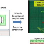
DRVerify is part of the iDRM design rule compiler platform from Sage DA, something that I have been personally involved with for the past three years. DRVerify is mainly used to verify third party design rule check (DRC) decks and ensure that they correctly, completely and accurately represent the design rule specification. In… Read More
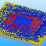
Power delivery networks (PDN) are the metal structures on a chip that delivers the power. In a high-end desktop SoC this might be delivering as much as 150W, and with voltages around 1V that means over 150 amps of current. Clearly getting the PDN correct is critical for a correctly functioning chip. One of the challenges to verifying… Read More


Quantum Computing Technologies and Challenges